EasyManua.ls Logo

Texas Instruments TMS320C6748 User Manual

Texas Instruments TMS320C6748
274 pages
To Next Page IconTo Next Page
To Previous Page IconTo Previous Page
Page #55 background image
55
TMS320C6748
www.ti.com
SPRS590G –JUNE 2009–REVISED JANUARY 2017
Submit Documentation Feedback
Product Folder Links: TMS320C6748
Device ComparisonCopyright © 2009–2017, Texas Instruments Incorporated
(1) I = Input, O = Output, I/O = Bidirectional, Z = High impedance, PWR = Supply voltage, GND = Ground, A = Analog signal.
Note: The pin type shown refers to the input, output or high-impedance state of the pin function when configured as the signal name
highlighted in bold. All multiplexed signals may enter a high-impedance state when the configured function is input-only or the configured
function supports high-Z operation. All GPIO signals can be used as input or output. For multiplexed pins where functions have different
types (ie., input versus output), the table reflects the pin function direction for that particular peripheral.
(2) IPD = Internal Pulldown resistor; IPU = Internal Pullup resistor; CP[n] = configurable pull-up/pull-down (where n is the pin group) using
the PUPDENA and PUPDSEL registers in the System Module. The pull-up and pull-down control of these pins is not active until the
device is out of reset. During reset, all of the pins associated with these registers are pulled down. If the application requires a pull-up,
an external pull-up can be used. For more detailed information on pullup/pulldown resistors and situations where external
pullup/pulldown resistors are required, see the Device Configuration section. For electrical specifications on pullup and internal pulldown
circuits, see the Device Operating Conditions section.
(3) This signal is part of a dual-voltage IO group (A, B or C). These groups can be operated at 3.3V or 1.8V nominal. The three groups can
be operated at independent voltages but all pins withina group will operate at the same voltage. Group A operates at the voltage of
power supply DVDD3318_A. Group B operates at the voltage of power supply DVDD3318_B. Group C operates at the voltage of power
supply DVDD3318_C.
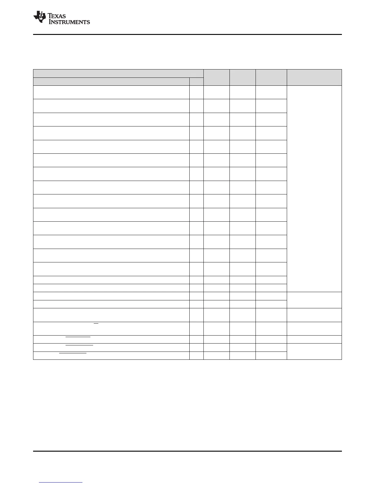
3.7.22 Universal Host-Port Interface (UHPI)
Table 3-26. Universal Host-Port Interface (UHPI) Terminal Functions
SIGNAL
TYPE
(1)
PULL
(2)
POWER
GROUP
(3)
DESCRIPTION
NAME NO.
VP_DIN[7] / UHPI_HD[15] / UPP_D[15] / RMII_TXD[1] /
PRU0_R31[29]
U18 I/O CP[26] C
UHPI data bus
VP_DIN[6] / UHPI_HD[14] / UPP_D[14] / RMII_TXD[0] /
PRU0_R31[28]
V16 I/O CP[26] C
VP_DIN[5] / UHPI_HD[13] / UPP_D[13] / RMII_TXEN /
PRU0_R31[27]
R14 I/O CP[26] C
VP_DIN[4] / UHPI_HD[12] / UPP_D[12] / RMII_RXD[1] /
PRU0_R31[26]
W16 I/O CP[26] C
VP_DIN[3] / UHPI_HD[11] / UPP_D[11] / RMII_RXD[0] /
PRU0_R31[25]
V17 I/O CP[26] C
VP_DIN[2] / UHPI_HD[10] / UPP_D[10] / RMII_RXER /
PRU0_R31[24]
W17 I/O CP[26] C
VP_DIN[1] / UHPI_HD[9] / UPP_D[9] / RMII_MHZ_50_CLK /
PRU0_R31[23]
W18 I/O CP[26] C
VP_DIN[0] / UHPI_HD[8] / UPP_D[8] / RMII_CRS_DV /
PRU1_R31[29]
W19 I/O CP[26] C
VP_DIN[15]_VSYNC / UHPI_HD[7] / UPP_D[7] / PRU0_R30[15] /
PRU0_R31[15]
V18 I/O CP[27] C
VP_DIN[14]_HSYNC / UHPI_HD[6] / UPP_D[6] / PRU0_R30[14] /
PRU0_R31[14]
V19 I/O CP[27] C
VP_DIN[13]_FIELD / UHPI_HD[5] / UPP_D[5] / PRU0_R30[13] /
PRU0_R31[13]
U19 I/O CP[27] C
VP_DIN[12] / UHPI_HD[4] / UPP_D[4] / PRU0_R30[12] /
PRU0_R31[12]
T16 I/O CP[27] C
VP_DIN[11] / UHPI_HD[3] / UPP_D[3] / PRU0_R30[11] /
PRU0_R31[11]
R18 I/O CP[27] C
VP_DIN[10] / UHPI_HD[2] / UPP_D[2] / PRU0_R30[10] /
PRU0_R31[10]
R19 I/O CP[27] C
VP_DIN[9] / UHPI_HD[1] / UPP_D[1] / PRU0_R30[9] / PRU0_R31[9] R15 I/O CP[27] C
VP_DIN[8] / UHPI_HD[0] / UPP_D[0] / GP6[5] / PRU1_R31[0] P17 I/O CP[27] C
PRU0_R30[29] / UHPI_HCNTL0 / UPP_CHA_CLOCK / GP6[11] U17 I CP[24] C
UHPI access control
PRU0_R30[28] / UHPI_HCNTL1 / UPP_CHA_START / GP6[10] W15 I CP[24] C
PRU0_R30[27] / UHPI_HHWIL / UPP_CHA_ENABLE / GP6[9] U16 I CP[24] C
UHPI half-word
identification control
PRU0_R30[26] / UHPI_HRW / UPP_CHA_WAIT /
GP6[8]/PRU1_R31[17]
T15 I CP[24] C UHPI read/write
VP_CLKIN0 / UHPI_HCS / PRU1_R30[10] / GP6[7] / UPP_2xTXCLK W14 I CP[25] C UHPI chip select
VP_CLKIN1 / UHPI_HDS1 / PRU1_R30[9] / GP6[6] / PRU1_R31[16] V15 I CP[25] C
UHPI data strobe
CLKOUT / UHPI_HDS2 / PRU1_R30[13] / GP6[14] T18 I CP[22] C

Table of Contents

Question and Answer IconNeed help?

Do you have a question about the Texas Instruments TMS320C6748 and is the answer not in the manual?

Texas Instruments TMS320C6748 Specifications

General IconGeneral
BrandTexas Instruments
ModelTMS320C6748
CategoryControl Unit
LanguageEnglish

Summary

Device Overview

Features

Lists the key features of the TMS320C674x Fixed- and Floating-Point VLIW DSP.

Description

Functional Block Diagram

Device Comparison

Device Characteristics

Overview of C6748 hardware features, peripherals, on-chip memory, and package type.

Memory Map Summary

Pin Assignments

Pin Multiplexing Control

Terminal Functions

Device Reset, NMI and JTAG Terminal Functions

Details terminal functions for RESET, NMI, and JTAG signals.

External Memory Interface A (EMIFA) Terminal Functions

Details terminal functions for the External Memory Interface A.

DDR2/mDDR Controller Terminal Functions

Details terminal functions for the DDR2/mDDR Memory Controller.

Serial Peripheral Interface Modules (SPI) Terminal Functions

Details terminal functions for SPI0 and SPI1 modules.

Programmable Real-Time Unit (PRU) Terminal Functions

Details terminal functions for the Programmable Real-Time Unit.

Boot

Details boot mode selection terminal functions.

Inter-Integrated Circuit Modules(I2C0, I2C1) Terminal Functions

Details terminal functions for I2C0 and I2C1 modules.

Multichannel Audio Serial Ports (McASP) Terminal Functions

Details terminal functions for McASP modules.

Multichannel Buffered Serial Ports (McBSP) Terminal Functions

Details terminal functions for McBSP modules.

Universal Serial Bus Modules (USB0, USB1) Terminal Functions

Details terminal functions for USB0 and USB1 modules.

Ethernet Media Access Controller (EMAC) Terminal Functions

Details terminal functions for the EMAC module.

Multimedia Card/Secure Digital (MMC/SD) Terminal Functions

Details terminal functions for MMC/SD card interfaces.

Liquid Crystal Display Controller(LCD) Terminal Functions

Details terminal functions for the LCD controller.

Serial ATA Controller (SATA) Terminal Functions

Details terminal functions for the SATA controller.

Universal Host-Port Interface (UHPI) Terminal Functions

Details terminal functions for the UHPI interface.

Universal Parallel Port (uPP) Terminal Functions

Details terminal functions for the Universal Parallel Port.

Video Port Interface (VPIF) Terminal Functions

Details terminal functions for the Video Port Interface.

Supply and Ground Terminal Functions

Details terminal functions for supply and ground pins.

Device Configuration

Boot Modes

Describes the various boot modes supported by the internal DSP ROM bootloader.

Pullup/Pulldown Resistors

Specifications

Absolute Maximum Ratings Over Operating Junction Temperature Range

Specifies the absolute maximum ratings for voltage and temperature.

Handling Ratings

Details handling precautions, including ESD voltage ratings.

Recommended Operating Conditions

Specifies recommended operating conditions for supply voltage and junction temperature.

Electrical Characteristics Over Recommended Ranges of Supply Voltage and Operating Junction Temperature

Details electrical characteristics over recommended operating ranges.

Power Supplies

Power-On Sequence

Describes the required order for powering on the device's various supplies.

Reset

Power-On Reset (POR)

Explains the Power-On Reset behavior and its effects on device logic and pins.

Reset Electrical Data Timings

Crystal Oscillator or External Clock Input

Clock PLLs

Enhanced Direct Memory Access Controller (EDMA3)

EDMA3 Peripheral Register Descriptions

Describes the EDMA3 Channel Controller and Transfer Controller registers.

Interrupts

DSP Interrupts

Details the C674x DSP interrupt controller, prioritized interrupts, and registers.

Power and Sleep Controller (PSC)

Memory Protection Units

MMC / SD / SDIO (MMCSD0, MMCSD1)

Serial ATA Controller (SATA)

Multichannel Audio Serial Port (McASP)

Multichannel Buffered Serial Port (McBSP)

Serial Peripheral Interface Ports (SPI0, SPI1)

Inter-Integrated Circuit Serial Ports (I2C)

Universal Asynchronous Receiver/Transmitter (UART)

Universal Serial Bus OTG Controller (USB0) [USB2.0 OTG]

Universal Serial Bus Host Controller (USB1) [USB1.1 OHCI]

Ethernet Media Access Controller (EMAC)

LCD Controller (LCDC)

Host-Port Interface (UHPI)

Universal Parallel Port (uPP)

Video Port Interface (VPIF)

Enhanced Capture (eCAP) Peripheral

Real Time Clock (RTC)

General-Purpose Input/Output (GPIO)

Programmable Real-Time Unit Subsystem (PRUSS)

Emulation Logic

Electrostatic Discharge Caution

Related product manuals