5.2 Device Identification Settings
These settings are used to distinguish which device is detected in a system. These settings cannot be changed
after device startup.
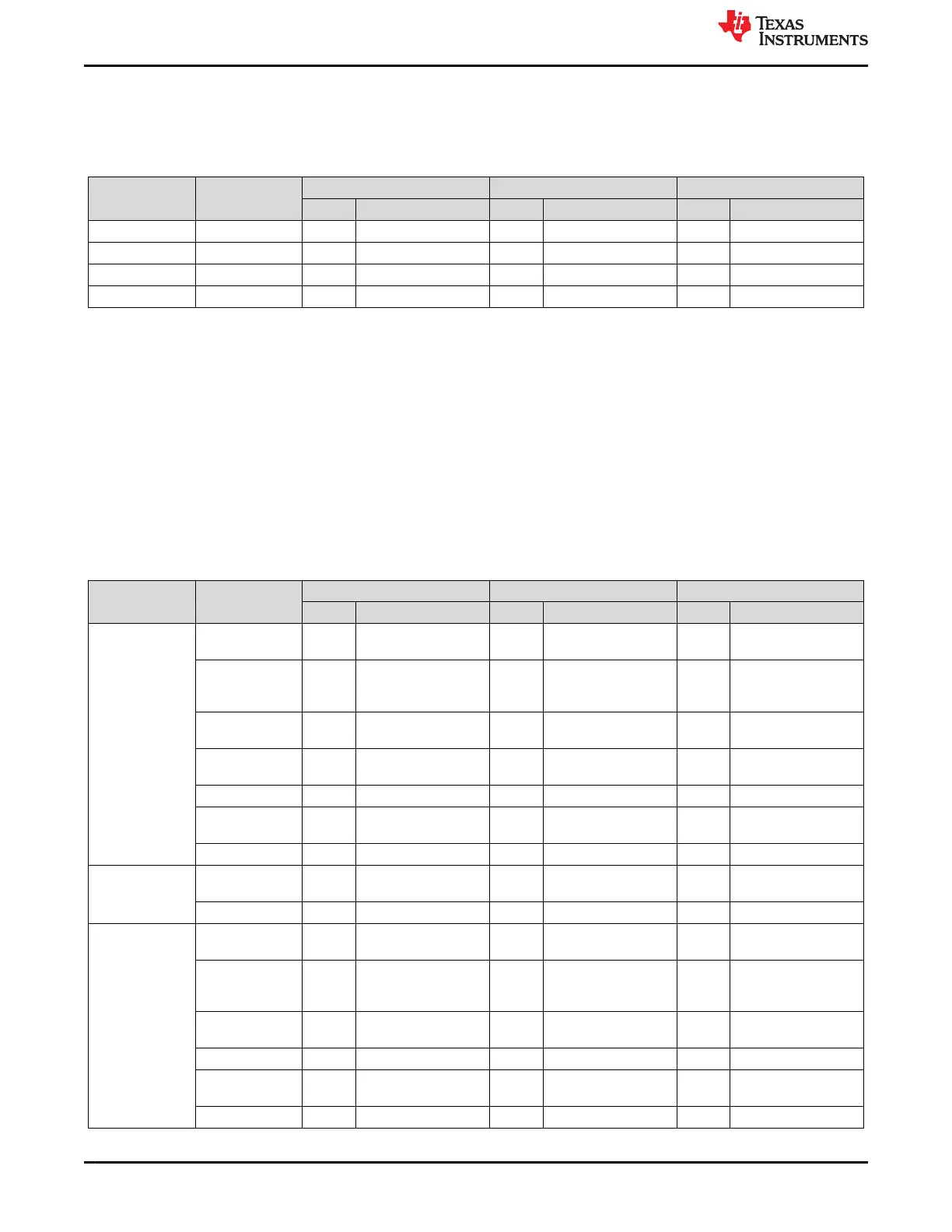
Table 5-2. Device Identification NVM Settings
Register Name Field Name
TPS65941120-Q1 TPS65941421-Q1 LP876411B5-Q1
Value Description Value Description Value Description
DEV_REV DEVICE_ID 0x82 0x82 0x86
NVM_CODE_1 TI_NVM_ID 0x20 0x21 0xb5
NVM_CODE_2 TI_NVM_REV 0x4 0x2 0x2
PHASE_CONFIG MP_CONFIG 0x0 4+1 0x1 1+1+1+1+1 0x0 4
5.3 BUCK Settings
These settings detail the voltages, configurations, and monitoring of the BUCK rails stored in the NVM. All these
settings can be changed though I
2
C after startup. Some settings, typically the enable bits, are also changed by
the PFSM, as described in Section 6.3.
After the Section 6.3.8 sequence has completed, the BUCKx_EN bit is set for BUCK1 and BUCK5 in the
TPS65941120-Q1. BUCKx_EN is set for the BUCK1, BUCK3, BUCK4 and BUCK5 in the TPS65941421-Q1.
BUCKx_EN is set for the BUCK1 in the LP876411B5-Q1. The BUCKx_VMON_EN bit is set for BUCK1, BUCK3
and BUCK5 in the TPS65941120-Q1. The BUCKx_VMON_EN bit is set for BUCK1, BUCK3, BUCK4 and
BUCK5 in the TPS65941421-Q1. The BUCKx_VMON_EN bit is set for BUCK1, BUCK3 and BUCK4 in the
LP876411B5-Q1. The BUCKx_RV_SEL bit is cleared for all BUCKs. The other bits remain unchanged, but are
still accessible via I
2
C.
Table 5-3. BUCK NVM Settings
Register Name Field Name
TPS65941120-Q1 TPS65941421-Q1 LP876411B5-Q1
Value Description Value Description Value Description
BUCK1_CTRL BUCK1_EN 0x0 Disabled; BUCK1
regulator
0x0 Disabled; BUCK1
regulator
0x0 Disabled; BUCK1
regulator
BUCK1_FPWM 0x1 PWM operation only. 0x0 PFM and PWM
operation (AUTO
mode).
0x1 PWM operation only.
BUCK1_FPWM_
MP
0x0 Automatic phase
adding and shedding.
0x0 Automatic phase
adding and shedding.
0x0 Automatic phase
adding and shedding.
BUCK1_VMON_
EN
0x0 Disabled; OV, UV, SC
and ILIM comparators.
0x0 Disabled; OV, UV, SC
and ILIM comparators.
0x0 Disabled; OV, UV, SC
and ILIM comparators.
BUCK1_VSEL 0x0 BUCK1_VOUT_1 0x0 BUCK1_VOUT_1 0x0 BUCK1_VOUT_1
BUCK1_PLDN 0x1 Enabled; Pull-down
resistor
0x1 Enabled; Pull-down
resistor
0x1 Enabled; Pull-down
resistor
BUCK1_RV_SEL 0x1 Enabled 0x1 Enabled 0x1 Enabled
BUCK1_CONF BUCK1_SLEW_R
ATE
0x3 5.0 mV/μs 0x3 5.0 mV/μs 0x3 5.0 mV/μs
BUCK1_ILIM 0x5 5.5 A 0x5 5.5 A 0x7 7.5 A
BUCK2_CTRL BUCK2_EN 0x0 Disabled; BUCK2
regulator
0x0 Disabled; BUCK2
regulator
0x0 Disabled; BUCK2
regulator
BUCK2_FPWM 0x1 PWM operation only. 0x0 PFM and PWM
operation (AUTO
mode).
0x1 PWM operation only.
BUCK2_VMON_
EN
0x0 Disabled; OV, UV, SC
and ILIM comparators.
0x0 Disabled; OV, UV, SC
and ILIM comparators.
0x0 Disabled; OV, UV, SC
and ILIM comparators.
BUCK2_VSEL 0x0 BUCK2_VOUT_1 0x0 BUCK2_VOUT_1 0x0 BUCK2_VOUT_1
BUCK2_PLDN 0x1 Enabled; Pull-down
resistor
0x1 Enabled; Pull-down
resistor
0x1 Enabled; Pull-down
resistor
BUCK2_RV_SEL 0x1 Enabled 0x0 Disabled 0x1 Enabled
Static NVM Settings www.ti.com
16 TPS65941120-Q1, TPS65941421-Q1 and LP876411B5-Q1 PMIC User Guide
for J721S2, PDN-0A
SLVUCJ9 – FEBRUARY 2023
Submit Document Feedback
Copyright © 2023 Texas Instruments Incorporated
 Loading...


