Note that the settings of the programmable address registers (24B ∼ 26A) are stored
in nonvolatile EEPROM. Therefore, do not write to any of these registers more than
10,000 times. Typically, these registers would only be written to once, when the
inverter and Modbus network are first commissioned. Also note that when the Modbus
interface board is first installed, the default contents of these registers are initialized to
0 (“unconfigured address”). Attempts to read from or write to programmable data
registers (26B ∼ 28A) which have corresponding programmable address registers set
to “unconfigured address” will generate ILLEGAL DATA ADDRESS exceptions
(Modbus exception code 02).
8.3 Loss of Communications Timer Function
A configurable "loss of communications" timer function is provided, which can detect
communication losses and perform certain actions if a valid packet is not received
and processed within a set time period.
Register 1D0 sets the loss of communication time value (adjustable from 100ms to
60.000s in 1ms increments, factory setting = 1.000s). If a valid (exception-free)
reception-response (or exception-free broadcast) does not take place within this time
limit, the timer will expire. If the timer expires, 5 possible actions can occur, as set by
the value of register 1D1 (loss of communications action):
Setting 0 is the default setting; when a communications timeout occurs, no action will
be taken.
For setting 1 (flash "COMM" on LCD display only), this condition will continue until the
next exception-free network packet is received and responded to (if the packet is a
broadcast, no response will be sent). The warning condition will then be removed and
the timer value reset.
For setting 2 (flash "COMM" on LCD display, stop inverter with decelerated stop), the
"COMM" warning will act as described in setting 1, but the inverter stop condition will not
be reset when an exception-free network packet is once again received. Note that
although the inverter stop condition is set, this only causes the inverter to actually stop
if parameter COMMAND MODE SELECTION in GROUP:UTILITY PARAMETERS is set
to 3 (communication option input valid). The inverter will then remain stopped until
commanded otherwise by the Modbus master.
Setting 3 does not depend on the COMMAND MODE SELECTION or FREQUENCY
MODE SELECTION parameters. Note that the “OPTION PCB ERROR” trip can only
be cleared locally at the inverter.
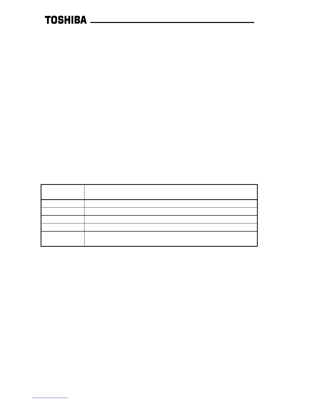
Register 1D1
Setting
Action Taken Upon Timeout
0 (default) No action: ignore timeout
1 Flash "COMM" on LCD display only
2 Flash "COMM" on LCD display, stop inverter with decelerated stop
3 Trip "OPTION PCB ERROR" (inverter must be reset locally)
4 Flash "COMM" on LCD display, set option frequency command to
UPPER LIMIT FREQUENCY (CAUTION!)
 Loading...