6. CAUTION! The option ROM PCB assembly and interface board are
static-sensitive devices. Standard electrostatic-sensitive component handling
precautions should be observed. Locate the option ROM connector, labeled
CN41, on the lower-left side of the control PCB. Line up the connector on the back
of the option ROM PCB with CN41. Install the option ROM by pressing gently but
firmly on the option ROM PCB until a slight “click” is felt. Verify that the option
ROM PCB is seated properly and firmly in CN41. If the option ROM connector
does not appear to be mating with CN41 properly, verify that the ROM is oriented
properly and that there are no obstructions in either connector.
7. Set the Modbus interface board's DIP switches for the desired communication
parameters (refer to section 6).
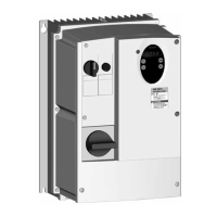
8. Install the 4 nylon standoffs into the holes provided in the control board support
bracket (refer to Figure 2).
9. Install the Modbus network cable through the access holes at the bottom of the
inverter and route the cable in order to make connections to the interface board
connector (TB1). Take care to not route the cable near any sharp edges or in
positions where it may be pinched.
10. Connect the Modbus cable to the interface board connector (TB1).
CAUTION! Extremely high voltages exist in the area near the Modbus
interface board and connector (TB1). Ensure that no stray wires (such as the
shield on the Modbus communications wire) come into contact with any internal
standoff mounting holes
Figure 2: G3 with front cover and operation panel support bracket
removed
 Loading...