15
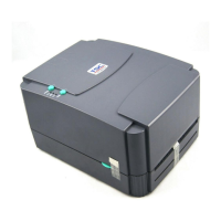
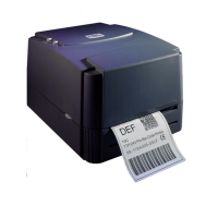
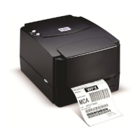
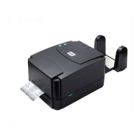
TTP-243 Bar Code Printer
Service Manua
l
3.2 MCU Pin Description
Pin Name Input/Output Function
Vcc, Vss Power supply
Supply 5V±10% to Vcc and 0V to Vss.
CNVss CNVss input Input This pin controls the processor mode.
Connect to Vss for single-chip mode,
and to Vcc for external ROM types.
/RESET Reset input Input To enter the reset state, this pin must be
kept at “L” condition, and maintained for
the required time.
X
IN
Clock input Input
X
OUT
Clock output Output
These are I/O pins of internal clock
generating circuit. Connect a ceramic or
quartz crystal resonator between X
IN
and
X
OUT
. When an external clock is used,
the clock source should be connected to
the X
IN
pin, and the X
OUT
pin and should
be left open.
/E Enable output Output Data/instruction read and data write are
performed when output from this pin is
“L”.
BYTE Bus width
selection input
Input In memory expansion mode or
microprocessor mode, this pin
determines whether the external data
bus is 8-bit width or 16-bit width. The
width is 16 bits for “L” signal input and 8
bits for “H” signal input.
/HOLD /HOLD input
pin
Input This is an input pin for the /HOLD
request signal.
/RDY /RDY input pin
Input
This is an input pin for the /RDY signal.
ψ1 Clock ψ1
output
Output
This is theψ1 output pin which is
divided the clock X
IN
pin by 2.
ST0, ST1 Status signal
output pin
Output The bus use status output is generated
in 2-bit code
AVcc, AVss Analog supply
input
Power supply for the A-D converter.
Connect AV
CC
and AV
SS
to V
SS
externally.
V
REF
Reference
voltage input
Input This is reference voltage input pin for
the A-D converter.
A0/MA0~
A7/MA7
Address
low-order/DRA
M address
Output This is an output pin for the 8 low-order
bits of addresses. When the DRAM is to
be accessed, the row and column
addresses are generated by means of
time division multiplexing.
 Loading...