10 www.xilinx.com FMC XM105 Debug Card User Guide
UG537 (v1.2) September 24, 2010
Chapter 1: XM105
Board Technical Description
The XM105 provides a number of multi-position headers and connectors which break out
the FPGA interface signals to and from the board interface. A serial IIC bus
reprogrammable LVDS clock source and a pair of SMA connectors provide differential
clock sources to the board FGPA. A 2-Kb serial IIC EEPROM is connected to the IIC
interface of the board providing non-volatile storage.
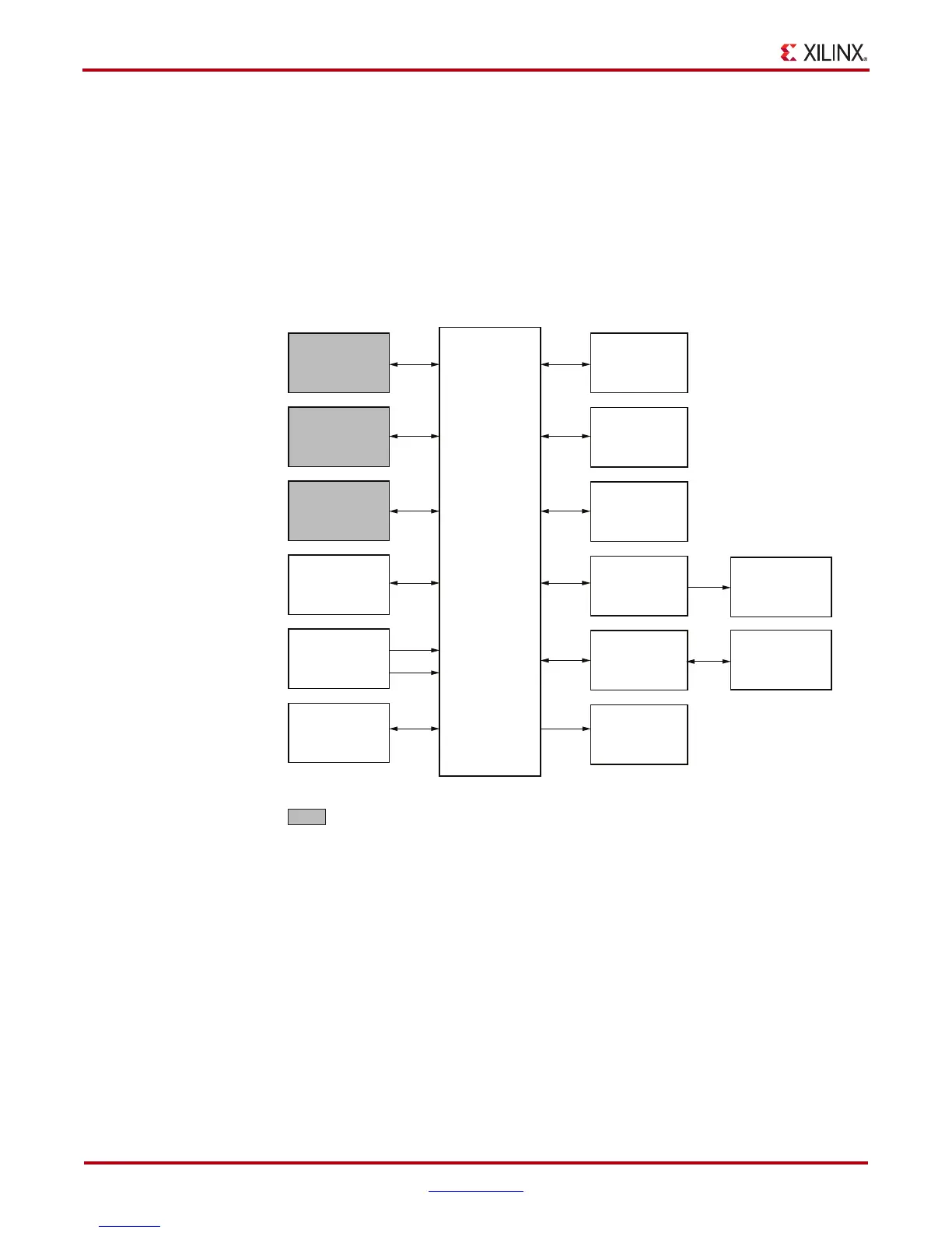
Figure 1-2 shows a block diagram of the XM105. The gray shaded blocks are only available
when the board interface is a high pin count board interface. All other interfaces are
available for low pin count board applications.
X-Ref Target - Figure 1-2
Figure 1-2: XM105 Block Diagram
UG537_02_110509
J2 Header
2 x 20
J1 Header
2 x 20
J20 Header
2 x 8
J16 Header
2 x 6
J15 Header
1 x 6
Mictor P1
38 Position
Power Good
LEDs
User
LEDs
J19 Head
1 x 9 JTAG
J3 Header
2 x 20
J23 Header
2 x 6
J5 Header
1 x 9
FMC JTAG
SMA J9, J10
LVDS Clock
J17
FMC HPC
Interface
2 Kb
EEPROM
Requires board with FMC HPC support.
Downloaded from Elcodis.com electronic components distributor