FMC XM105 Debug Card User Guide www.xilinx.com 25
UG537 (v1.2) September 24, 2010
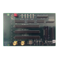
Board Technical Description
12. Mictor Connector P1
This 38-position connector contains an interface from the XM105 to 21 signals on the
board’s FMC LPC or FMC HPC interface. Four Mictor JTAG signals are wired to connector
J19. Connections between the mezzanine FMC HPC and connector P1 are defined in
Table 1-12. The Mictor connector is AMP part number 2-767004-2.
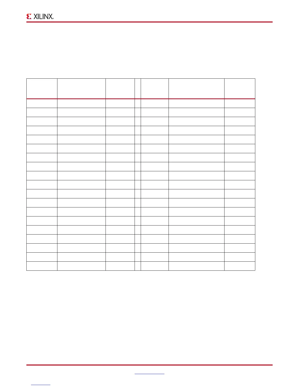
Table 1-12: Mezzanine FMC J17 to Mictor Connector P1 Pin Assignments
FMC HPC
Connector
J17 Pin
Signal Name
P1
Connector
(Odd Pins)
FMC HPC
Connector
J17 Pin
Signal Name
P1
Connector
(Even Pins)
–NC1NANC 2
–NC3NANC 4
– NC 5 G6 FMC_LA00_CC _P
(2)
6
–NC7NANC 8
–NC9NANC 10
NC MICTOR_TDO
(1)
11 VADJ 12
–NC13NANC 14
NC MICTOR_TCK
(1)
15 D9 FMC_LA01_CC _N
(2)
16
NC MICTOR_TMS
(1)
17 D8 FMC_LA01_CC _P
(2)
18
NC MICTOR_TDI
(1)
19 D15 FMC_LA09_N 20
– NC 21 D14 FMC_LA09_P 22
G13 FMC_LA08_N 23 H11 FMC_LA04_N 24
G12 FMC_LA08_P 25 H10 FMC_LA04_P 26
H14 FMC_LA07_N 27 G10 FMC_LA03_N 28
H13 FMC_LA07_P 29 G9 FMC_LA03_P 30
C11 FMC_LA06_N 31 H8 FMC_LA02_N 32
C10 FMC_LA06_P 33 H7 FMC_LA02_P 34
D12 FMC_LA05_N 35 C15 FMC_LA10_N 36
D11 FMC_LA05_P 37 C14 FMC_LA10_P 38
Notes:
1. Mictor JTAG
signals are available on 9-position connector J19.
2. Signal names with “_CC_” may be connected to FPGA clock capable pins on the board. See Xilinx board user guides for
additional information.
Downloaded from Elcodis.com electronic components distributor