FMC XM105 Debug Card User Guide www.xilinx.com 27
UG537 (v1.2) September 24, 2010
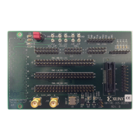
Board Technical Description
14. Clocks
Two clock sources (Table 1-14) are provided for FMC LPC and FMC HPC board
applications:
• Differential SMA connectors
• Si570 IIC LVDS clock
A pair of differential SMA connectors can be utilized to provide a high-precision
differential clock or a single-ended clock to the board. Virtex-6 FPGA and Spartan-6 FPGA
devices require single-ended clocks on the “P” input of an IOB pair. See Xilinx FPGA
documentation for additional information.
Consult Xilinx FMC- supported board user guide for interface voltages, I/O standard
support on FPGA clock pins; and to determine LVDS input clock termination
requirements, either on the printed-circuit board or using an IBUFGDS primitive for FPGA
on-chip termination.
A Silicon Labs Si570 IIC programmable clock source provides a low-jitter clock with a user-
programmable output frequency from 10 to 810 MHz. As shipped, the CLK0_M2C clock
frequency is 156.25 MHz. The component installed on the XM105 is factory programmed
with parameters in Table 1-15.
For additional information on this component, including reprogramming the clock
frequency through the IIC serial bus interface, consult the Silicon Labs Si570 Data Sheet at
https://www.silabs.com
.
Table 1-14: Clock Sources Routed to Mezzanine FMC HPC J17 Connector
FMC HPC
Connector J17 Pin
Signal Name Source
(1)
H4 CLK0_M2C_P
(2)
Si570 U2 pin 4
H5 CLK0_M2C_N
(2)
Si570 U2 pin 5
G2 CLK1_M2C_P SMA J9
G3 CLK1_M2C_N SMA J10
Notes:
1. Clock sources are available for FMC LPC and FMC HPC board
applications.
2. The Si570 provides a LVDS output clock.
Table 1-15: Characteristics of Si570 Component
Si570 Characteristic XM105
Output Format LVDS
Output Enable Polarity High
Temperature Stability 50 ppm
Frequency Range 10–810 MHz
Six-Digit Startup 156.250 MHz
Power Supply 3.3V
IIC Address x5D
Downloaded from Elcodis.com electronic components distributor
 Loading...