12 www.xilinx.com FMC XM105 Debug Card User Guide
UG537 (v1.2) September 24, 2010
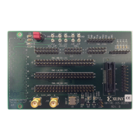
Chapter 1: XM105
9 40-pin header
(1)
J2: 20 pin x 2 row male header 8
10 40-pin header J1: 20 pin x 2 row male header 7
11 40-pin header
(1)
J3: 20 pin x 2 row male header 8
12 Mictor connector P1: 38 pin female Mictor connector 6
13 9-pin header
J19: 9 pin x 1 row male header with Mictor JTAG pins connected
between J19 and P1
6
14 Clocking
SMA connectors (J9, J10) and Silicon Labs Si570 IIC serial bus
reprogrammable LVDS clock source
9
15 2 Kb EEPROM
IIC compatible electrically erasable programmable memory
(EEPROM) with 2 Kb (256 bytes) of non-volatile storage.
2
16 Power Good LEDS
Power good LEDS for +12V, board to mezzanine card (PG_C2M) and
V
adjust
/3.3V
7
17 2-pin header
J18: 2 pins x 1 male header for GND connection to PG_M2C LPC
connector.
3
Notes:
1. Available only with FMC HPC board interfaces. Xilinx Virtex-6 FPGA ML605 evaluation board provides one FMC LPC and one
FMC HPC interface. Xilinx Spartan-6 FPGA SP601 and SP605 evaluation boards provide a single FMC LPC interface.
Table 1-2: XM105 Features (Cont’d)
Number Feature Notes
Schematic
Page
Downloaded from Elcodis.com electronic components distributor