VCU118 Board User Guide 30
UG1224 (v1.0) December 15, 2016
www.xilinx.com
Chapter 3: Board Component Descriptions
The VCU118 dual DDR4 80-bit memory component interfaces adhere to the constraints
guidelines documented in the “DDR3/DDR4 Design Guidelines” section of the UltraScale
Architecture-Based FPGAs Memory IP LogiCORE IP Product Guide (PG150) [Ref 4]. The
VCU118 board DDR4 memory component interface is a 40Ω impedance implementation.
For more information on the internal VREF, see the “Supply Voltages for the SelectIO Pins
VREF” and the “Internal VREF” sections in the UltraScale Architecture SelectIO Resources User
Guide (UG571) [Ref 3]. For more details about the Micron DDR4 component memory, see
the Micron MT40A256M16GE data sheet at the Micron website [Ref 18].
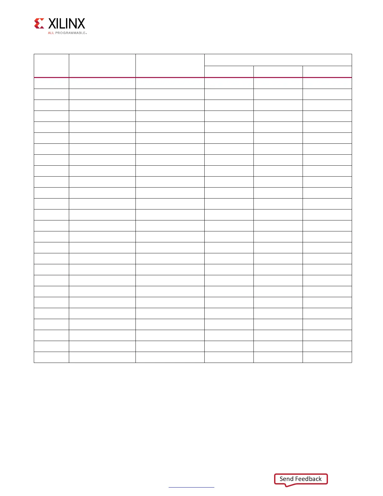
AN28 DDR4_C2_A4 SSTL12_DCI N3 A4 U135-U139
AM28 DDR4_C2_A5 SSTL12_DCI P8 A5 U135-U139
AP28 DDR4_C2_A6 SSTL12_DCI P2 A6 U135-U139
AP27 DDR4_C2_A7 SSTL12_DCI R8 A7 U135-U139
AN26 DDR4_C2_A8 SSTL12_DCI R2 A8 U135-U139
AM26 DDR4_C2_A9 SSTL12_DCI R7 A9 U135-U139
AR28 DDR4_C2_A10 SSTL12_DCI M3 A10/AP U135-U139
AR27 DDR4_C2_A11 SSTL12_DCI T2 A11 U135-U139
AV25 DDR4_C2_A12 SSTL12_DCI M7 A12/BC_B U135-U139
AT25 DDR4_C2_A13 SSTL12_DCI T8 A13 U135-U139
AR25 DDR4_C2_BA0 SSTL12_DCI N2 BA0 U135-U139
AU28 DDR4_C2_BA1 SSTL12_DCI N8 BA1 U135-U139
AU27 DDR4_C2_BG0 SSTL12_DCI M2 BG0 U135-U139
AV28 DDR4_C2_A14_WE_B SSTL12_DCI L2 WE_B/A14 U135-U139
AU26 DDR4_C2_A15_CAS_B SSTL12_DCI M8 CAS_B_A15 U135-U139
AV26 DDR4_C2_A16_RAS_B SSTL12_DCI L8 RAS_B/A16 U135-U139
AT26 DDR4_C2_CK_T DIFF_SSTL12_DCI K7 CK_T U135-U139
AT27 DDR4_C2_CK_C DIFF_SSTL12_DCI K8 CK_C U135-U139
AW28 DDR4_C2_CKE SSTL12_DCI K2 CKE U135-U139
AN25 DDR4_C2_ACT_B SSTL12_DCI L3 ACT_B U135-U139
BF29 DDR4_C2_PAR SSTL12_DCI P9 ALERT_B U135-U139
BB29 DDR4_C2_ODT SSTL12_DCI T3 PAR U135-U139
AY29 DDR4_C2_CS_B SSTL12_DCI K3 ODT U135-U139
AR29 DDR4_C2_ALERT_B SSTL12_DCI L7 CS_B U135-U139
BD35 DDR4_C2_RESET_B LVCMOS12 P1 RESET_B U135-U139
AY35 DDR4_C2_TEN SSTL12_DCI N9 TEN U135-U139
Table 3-3: DDR4 Memory 80-bit I/F C2 to FPGA U1 Banks 40, 41, and 42 (Cont’d)
FPGA (U1)
Pin
Schematic Net Name I/O Standard
Component Memory
Pin # Pin Name Ref. Des.