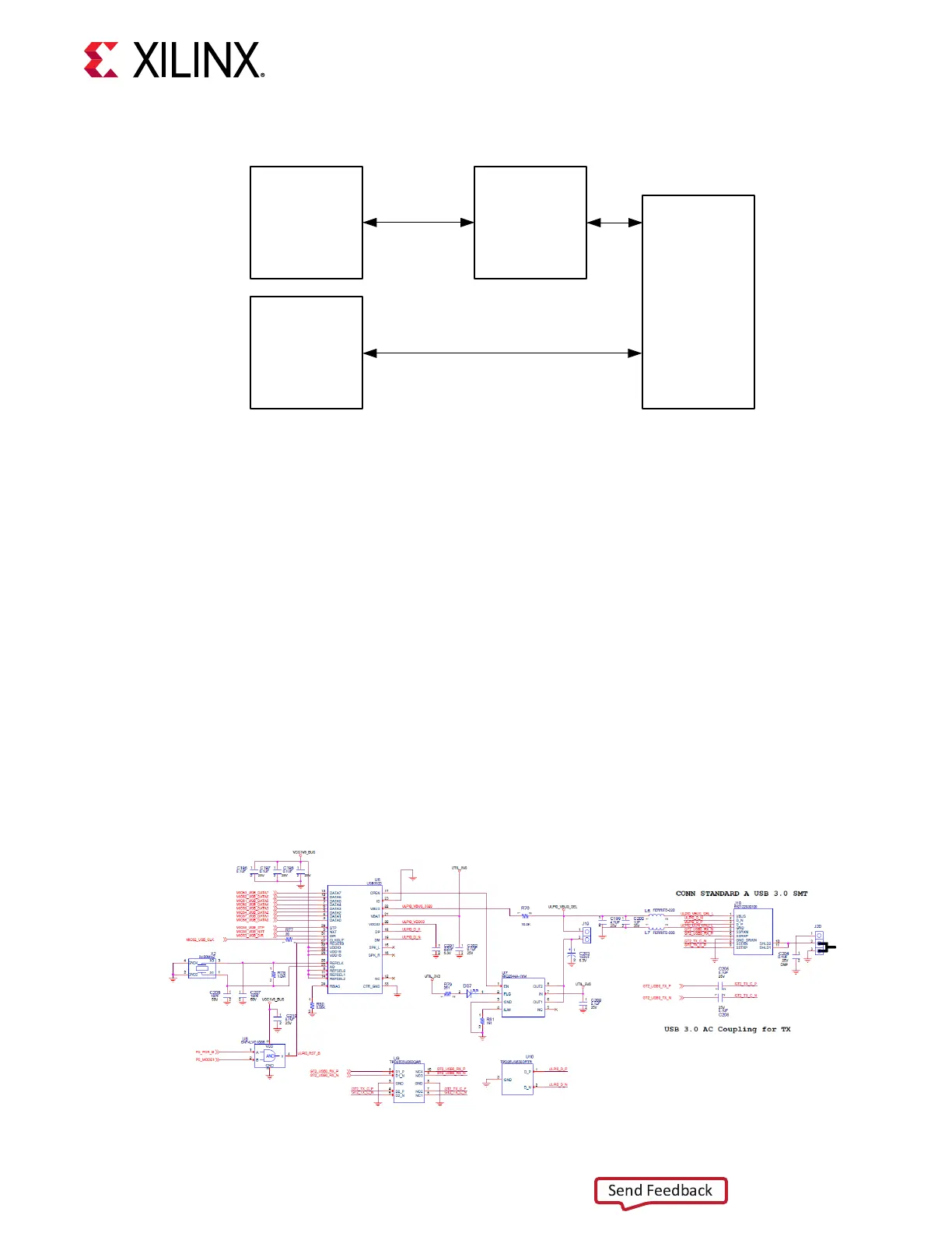
Figure 11: USB Interface
SM3320
USB2.0
USB
MIO
ULPI
GTR Tx, Rx
USB3
Connector
USB
GTR
X23650-032720
The USB3320 is clocked by a 24 MHz crystal (X2). See the Standard Microsystems Corporaon
USB3320 data sheet for clocking mode details.
The interface to the USB3320 PHY is implemented through the IP in the ZU48DR RFSoC
Processor System (PS). USB OTG support is available for USB 2.0. See Table 3 for USB 2.0 jumper
sengs.
Note: The shield for the USB 3.0 micro-B connector (J18) can be ed to GND by a jumper on header J20
pins 2-3 (default). The USB shield can oponally be connected through a series capacitor to GND by
installing a capacitor (body size 0402) at locaon C204 and jumping pins 1-2 on header J20.
The USB3320 ULPI U6 transceiver circuit (see the following gure) has a Micrel MIC2544 high-
side programmable current limit switch (U7). This switch has an open-drain output fault ag on
pin 2, which will turn on LED DS7 if overcurrent or thermal shutdown condions are detected.
DS7 is located adjacent to the USB J18 connector (Figure 2, callout 6).
The following gure shows the ULPI U6 transceiver circuit.
Figure 12: USB3320 ULPI USB 2.0 Transceiver Circuit
Chapter 3: Board Component Descriptions
UG1410 (v1.0) July 8, 2020 www.xilinx.com
ZCU208 Board User Guide 39

 Loading...