A
1
2
3
4
5
6
7
8
9
10
BCDEFGH I JK
L MN
RX-V1700/DSP-AX1700
106
★ All voltages are measured with a 10MΩ/V DC electronic voltmeter.
★ Components having special characteristics are marked s and must be replaced
with parts having specifications equal to those originally installed.
★ Schematic diagram is subject to change without notice.
FUNCTION 1/4
5.5
0
11.9
5.6
0
5.1
~0
0
2.3
5.1
4.2
5.0
0.1 0.1
4.9
11.2
5.1
5.6
4.9
4.9
4.9
4.9
4.9
4.9
4.9
0
0
0
0
0
0
5.1
0
3.3
0
0
5.0
5.0
5.0
5.1
5.1
-11.2
-11.2
5.1
-11.2
5.1
-11.2
5.1
-11.2
5.1
-11.2
5.1
-11.2
0
0
00
00
5.1
00
0
3.1
0
4.9
0.1
0
4.9
4.9
4.9
4.9
4.9
4.9
4.9
4.9
4.9
5.1
0
0
0
5.1
0
5.1
0
5.0
4.9
0
0.1
0.1
4.9
0.1
~
4.9
5.0
0
5.1
5.1
4.9
5.1
0.1
0.1
4.9
5.0
5.0
0.1
0.1
0.1
0
0
5.1
5.1
0
0
0
4.9
0
0
4.5
4.9
5.1
5.1
1.1
1.1
0.4
0
0.2
0.4 0.4
1.4
5.1
5.1
4.5
4.2
8.3 5.8 5.8
4.9
5.1
5.1
5.1
0
3.7
5.1
0
0
5.0
5.1
1.4
1.7
0.1
0
5.1
4.9
4.9
4.9
4.8
5.0
0.1
4.9
5.1
0
0
0
0
0
0
4.9
4.9
0
0
0
4.9
4.9
2.5
0
2.3
5.1
5.0
4.9
5.4
5.1
5.1
4.8
4.8
0
5.0
0.1
5.0
4.8
0.2
5.0
5.0
4.9
5.0
5.1
0
4.9
4.9
0
0
0
0
0
4.0
0
0
5.1
5.1
0.1
0.1
0
4.9
4.9
4.9
4.9
0
0
4.8
4.9
4.9
4.9
0
0
4.9
0
5.1
0
0
5.1
5.1
4.9
5.1
4.8
5.1
0.1
0.1
4.9
5.1
4.9
0
0
0
2.3
2.3
2.3
2.0
B-3
0
0
4.5
00.1
0
1.8
0
5.0
11.9
5.6
0.2
B-2
C-1
1
C-2
2
100/16
4.7K
47K
no-use
no-use
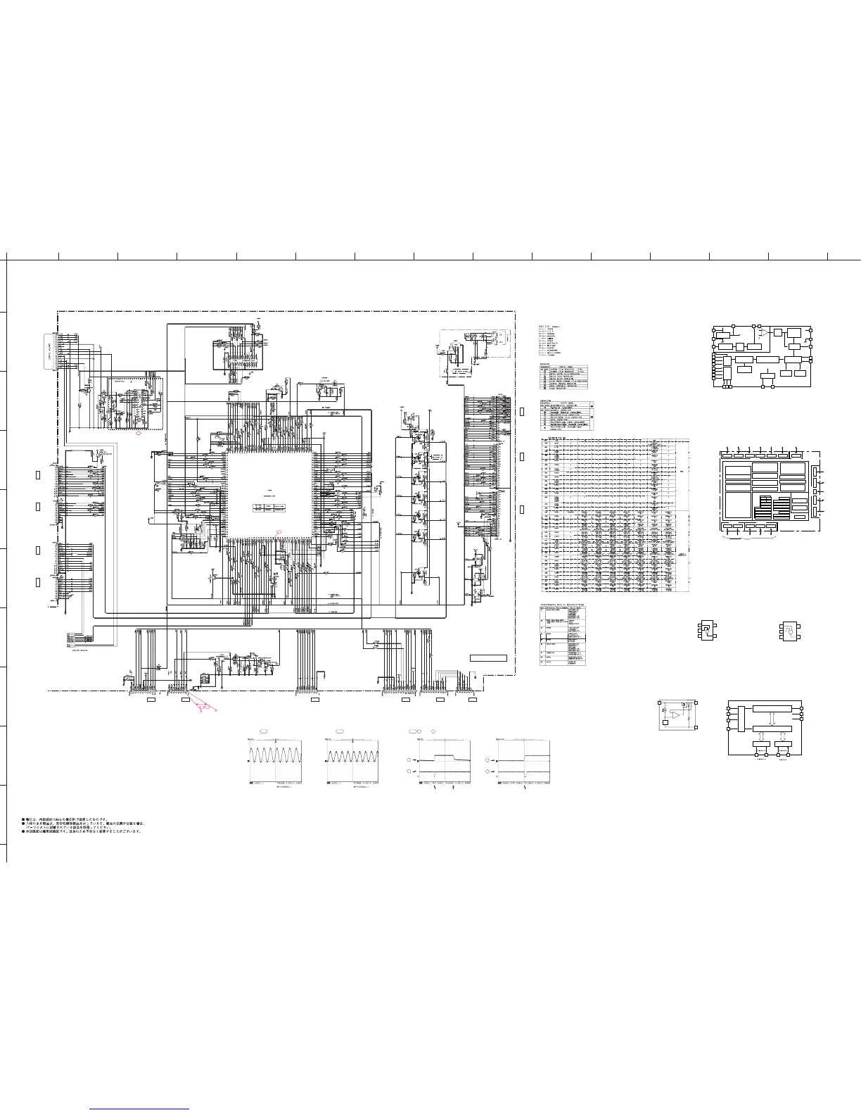
FUNCTION (1)
MICROPROCESSOR
(MAIN)
To FUNCTION 2/4
IC401: LC72722PM
RDS signal processor
Single chip 16/32-bit microprocessor
REFERENCE
VOLTAGE
57 kHz
bpf
(SCF)
CCB
TEST
PLL
(57 kHz)
ANTIALIASING
FILTER
SMOOTHING
FILTER
RAM
(24 BLOCK DATA)
ERROR CORRECTION
(SOFT DECISION)
SYNC / EC
CONTROLLER
SYNC
DETECT-1
DATA
DECODER
CLOCK
RECOVERY
(1187.5 Hz)
MEMORY
CONTROL
OSC/DIVIDER
VREF
CLK (4.332 MHz)
SYNC
DETECT-2
VDDA
VSSD
VDDD
RDS-ID
SYNC
SYR
VSSA
MPX IN
DO
CL
DI
CE
T1
T2
T3
T4
T5
T6
T7
X IN
VREF
FL OUT
C IN
X OUT
3
14
15
19
18
24
1 5 6
4
2
20
21
22
23
7
8
9
10
11 16 17 13 12
2
1
3
Vref
V
OUT
GND
V
IN
–
+
IC407: RH5RE58AA-T1-FA
Voltage regulator
Y4
B2
GND 3
IC405: SN74AHC1G08DCKR
2-input positive-AND gate
Vcc5A1
Y4
B2
GND 3
IC404, 406: SN74AHCT1G32DCKR
Single 2-input positive-OR gate
Vcc5A1
IC402: M30845FJGP
Port P0 Por t P1 Port P2 Por t P3 Po rt P4 Port P5 Port P6
Port P7
Port P14 Por t P15 Port P11 Port P12
Port P10Port P9Por t P8
P85
Port P13
R0H R0L
R1H R1L
R2
R3
A0
A1
FB
SB
NOTES:
1. Ports P11 to P1 5 are provided in th e 144-pin pack age only.
2. Includ ed in the 144-pin pa ckage only.
3. The suppl y voltage of M32C/ 84T (High-reli ability vers ion) must be V
CC1=VCC2.
FLG
INTB
ISP
USP
PC
SVF
SVP
VCT
Multiplier
M32C/80 series CPU Core
Clock Generation Circuit
XIN - XOUT
XCIN - XCOUT
On-chip Oscillator
PLL Frequenc y Synthesizer
A/D Converter:
1 circuit
Standard: 10 inputs
Maximum: 34 inputs
(2)
UART/Clock Synchronous Serial I/O:
5 channels
CRC Calculation Circuit (CCITT):
X
16
+X
12
+X
5
+1
X/Y Converter:
16 bits x 16 bits
D/A Converte r:
8 bits x 2 channels
Peripher al Functions
<VCC2
(3)
>
<
VCC1
(3)
>
<VCC1
(3)
>
ROM
RAM
Memory
<VCC1
(3)
>
<VCC2
(3)
>
78 58 8
(Note 1)
8
8
7
888888 8
8
DMACII
DMAC
Watchdog Timer (1 5 bits)
CAN Module: 1 channel
Intelligent I/O
Time Measurement: 8 channels
Waveform Generating: 8 channels
Communication Functions:
Clock Synchronous Serial I/O, UART,
HDLC Data Processing
Timer (16 bits )
Timer A: 5 channels
Timer B: 6 channels
Three-Phase Motor Control Circuit
IC403: LC709004A-TLM-E
I/O-expander for microcontroller
Control logic
port 0 I/O buffer
Serial/parallel converter/shift register
I/O control/output register
DIN
VDD
DOUT
VSS
CLK#
CS#
RES#
P00
P07
2
14
15
19
3
4
21
24 17
port 1 I/O buffer
P10
P17
15 8
POINT B-2 Pin 20 of IC402 POINT B-3 Pin 12 of IC401 POINT C-1 1 / Pin7, 2 / Pin8 of CB405
1+5M
AC cable ON AC cable OFF
/RES
2
1
2
AC cable ON
to FL (6)_W9501
Page 117
K3
to POWER (4)_W1
Page 112 H7
to POWER (3)_W9
Page 112 D2
to POWER (3)_CB18
Page 112 G7
to A-VIDEO_CB203
Page 114 I2
to DSP_CB504
Page 103 E2
to FL (5)_CB960
To TUNER
Page 118
K5
to FL (5)_CB972
Page 118 J5
to FL (3)_CB955
Page 118 J6
to FL (3)_CB952
Page 118 J6
to FL (2)_CB969
Page 118
F6
to FL (2)_CB962
Page 118 E6
to FL (2)_CB958
Page 118 C6
 Loading...