A4-12
IM 34M06H62-02E 2nd Edition : June 2008-00
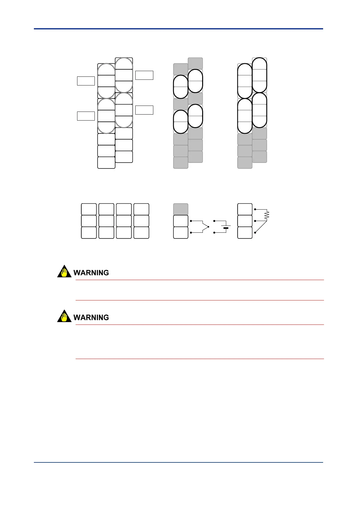
Terminal Diagram and Wiring Example for F3CU04-1S
2
4
6
8
1
3
5
7
IN1
IN3
IN2
IN4
10
12
14
16
18
9
11
13
15
17
NC
3+
NC
3-
NC
NC
4+
2+
2-
4-
NC
3b
3B
3A
2A
2b
4b
4B
2B
4A
NC
1+
1-
1A
1b
1B
NC
NC
NC
NC
NC
NC
NC
NC
NC
NC
IN1 IN3IN2 IN4
NC
+
-
A
b
B
8
10
12
7
9
11
2
4
6
1
3
5
+
-
b) Input Terminal Wiring Diagram for F3CU04-1S
a) Terminal Assignment
Diagram for F3CU04-1S
For thermocouple and
DC voltage input
For RTD input
Figure A4.10 Terminal Wiring Diagram
No wire must be connected to the terminals marked "NC" in the terminal assignment or
terminal wiring diagram. Otherwise, the module will not function normally.
All output terminals of F3CU04-1S are located on the right terminal block. Terminals 13-18
are not output terminals on F3CU04-1S, but are output terminals on F3CU04-0S. No wire
must be connected to these terminals on F3CU04-1S. Otherwise, the module will not
function normally.
 Loading...