JOHNSON CONTROLS
21
SECTION 2 - PRODUCT DESCRIPTION
FORM 201.23-NM2
ISSUE DATE: 09/25/2020
2
The power section of the drive is composed of four ma-
jor blocks consisting of an AC to DC rectifier section
with accompanying pre-charge circuit, a DC link filter
section, a three phase DC to AC inverter section, and
an output suppression network.
The AC to DC rectifier utilizes a semi-converter formed
by the connection of three SCR/diode modules (1SCR
through 3SCR) in a three phase bridge configuration.
The modules are mounted on a liquid cooled heatsink.
Use of the semi-converter configuration permits im-
plementation of a separate pre-charge circuit to limit
the flow of current into the DC link filter capacitors
when the drive is switched on and it also provides a
fast disconnect from the power mains when the drive is
switched off. When the drive is turned off, the SCR's in
the semi-converter remain in a non-conducting mode
and the DC link filter capacitors remain uncharged.
When the drive is commanded to run, the DC link filter
capacitors are slowly charged via the semi-converter.
The SCR’s are then gated fully on.
Three power fuses (1FU - 3FU), an optional circuit
breaker (1SW) and a standard 5% impedance minimum
3-phase line reactor connect the AC to DC converter to
the incoming power. Very fast semiconductor power
fuses are utilized to ensure that the SCR/diode module
packages do not rupture if a catastrophic failure were
to occur on the DC link. The SCR Trigger Board pro-
vides the gating pulses for the SCR’s as commanded by
the VSD Logic Board.
The DC Link filter section of the drive consists of a
group of electrolytic filter capacitors (C1-C6). This
capacitor bank effectively smoothes the ripple voltage
from the AC to DC rectifier while simultaneously pro-
viding a large energy reservoir for use by the DC to
AC inverter section of the drive. In order to achieve
the required voltage capability for the capacitor por-
tion of the filter, filter capacitor “banks” are formed by
connecting two groups of parallel capacitors in series
to form a capacitor “bank”. In order to assure an equal
sharing of the voltage between the series connected ca-
pacitors and to provide a discharge means for the ca-
pacitor bank when the VSD is powered off, “bleeder”
resistors (1RES and 2RES) are connected across the
capacitor banks.
Variable Speed Drive (VSD)
The VSD (variable speed drive) is a liquid cooled, tran-
sistorized, PWM inverter, which provides speed con-
trol to vary the speed of 2, 3 or 4 compressor motors.
The VSD changes the duration of the voltage pulses
supplied to the motor to enable control of compressor
speed to match the system load. A PWM generator, on
the VSD Logic Board, with a switching frequency of
3125 Hz modulates the voltage signal to provide a rela-
tively pulses constant V/F ratio. In some cases, the V/F
ratio is slightly modified to provide additional torque
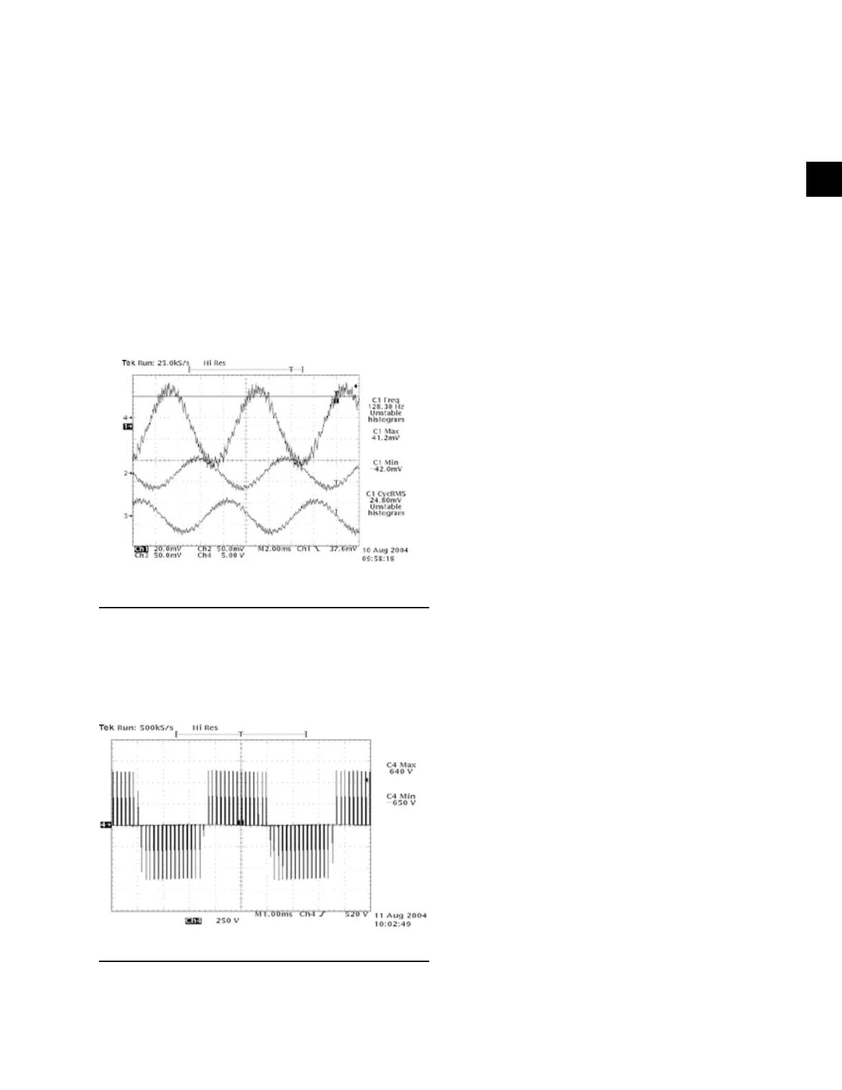
to the motor. Sample 3 phase current waveforms are
shown in Figure 3 on page 21 to show the sinusoidal
characteristics of the current drawn by the compressor
motors.
FIGURE 3 - PWM CURRENT WAVEFORM
LD10479
A Sample PWM voltage waveforms is shown in Figure
4 on page 21. The pulses near the sides of the rectan-
gular groups of waves are notably narrower, represent-
ing the lower voltage of a sinusoidal waveform as it
rises or falls from the “0” crossing.
FIGURE 4 - PWM VOLTAGE WAVEFORM
LD10480
 Loading...