Appendix
262
1SVC 440 795 M0100
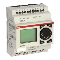
CL-LS...DC2,CL-LE...DC2, CL-LM...DC2
CL-LSR...DC2,
CL-LST...DC2
CL-LER...DC2,
CL-LET...DC2
CL-LMR...DC2,
CL-LMT...DC2
Digital inputs
Quantity 8 12 12
Inputs usable as analog
inputs
I7, I8 I7, I8, I11, I12
Status display LCD (if provided)
Potential isolation
To power supply No No No
Between each other No No No
To the outputs Yes Yes Yes
Rated voltage
Nominal value 24 V DC 24 V DC 24 V DC
At state ”0” < 5 V DC (I1 to I8) < 5 V DC (R1 to R12) < 5 V DC (I1 to I12)
At state ”1” > 8 V DC (I7, I8) > 8 V DC
(I7, I8, I11, I12)
> 15 V DC
(I1 to I6)
> 15 V DC
(R1 to R12)
> 15 V DC
(I1 to I6, I9, I10)
Input current for state “1” 3.3 mA at 24 V DC
(I1 to I6)
3.3 mA at 24 V DC
(R1 to R12)
3.3 mA at 24 V DC
(I1 to I6, I9, I10)
I7, I8 (CL-LM...DC2.
also I11, I12)
2.2 mA at 24 V DC 2.2 mA at 24 V DC
Delay time for 0 to 1
Debounce ON 20 ms 20 ms 20 ms
Debounce OFF
CL-LS...DC2 I1 to I8
CL-LE...DC2 R1 to R12
CL-LM...DC2 I1 to I12
Normally 0.25 ms
 Loading...