2-5
Assembly-Level Troubleshooting with Block Diagrams
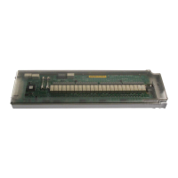
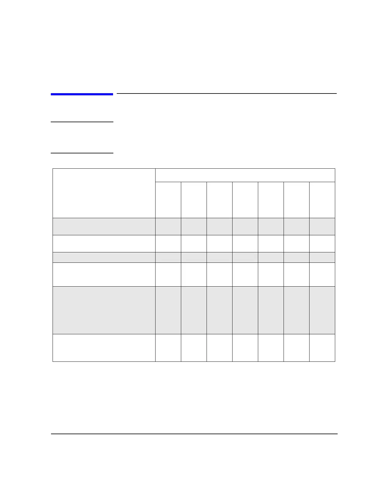
A9 Output Board
A9 Output Board
NOTE: The node voltages given in the following table are approximate values based on a sample
of signal generators. Your signal generator may not reflect these exact values. Additionally,
the resolution of these values varies from node to node. As a guideline, interpret your
measurements based on the number of decimal places shown for the expected voltage.
A9 Output Board Abus Nodes (1 of 2)
Test Conditions
Node Voltages (Corrected Values in Vdc)
ALC_MOD
BURST_MOD
ALC_DET
POW_REF_1
POW_REF_2
LOOP_INT
PTAT
PRESET; 0 dBm; RF On; No Modulation 0.7 19 0.08 1.2 0.5 1 8.5 to
9.9
PRESET; 0 dBm; RF Off; No Modulation 0.1 19 0.0 1.2 0.5 10 8.5 to
10.9
PRESET; 20 dBm; RF On (Unleveled) 20 19 0.4 0.4 1 12
Frequency Set to heterodyne Band;
PRESET; Frequency 249.9 MHz; 0 dBm;
RF On; No Modulation
0.4 19 0.05 1.1 0.3 0.0 8.5 to
10.9
+5.0 Vdc applied to Q INPUT:
PRESET; 0 dBm; RF
On; I/Q On; I/Q
Source EXT I/Q; I Input = No Connection;
Burst Envelope On; If 0.5Vdc is applied to
Q INPUT, the Q node changes to negative
voltage
0.9 (20
w/ no Q
Input)
4.8 0.08
(0.1 w/
no Q
Input)
1.3
(12 w/
no Q
Input)
+1 Vdc Applied to EXT 1 INPUT:
PRESET; 0 dBm; RF On; AM On;
AM Depth 100%; AM Source Ext 1 DC
 Loading...