2-13
Assembly-Level Troubleshooting with Block Diagrams
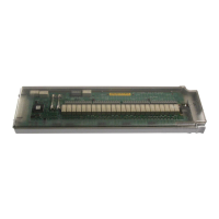
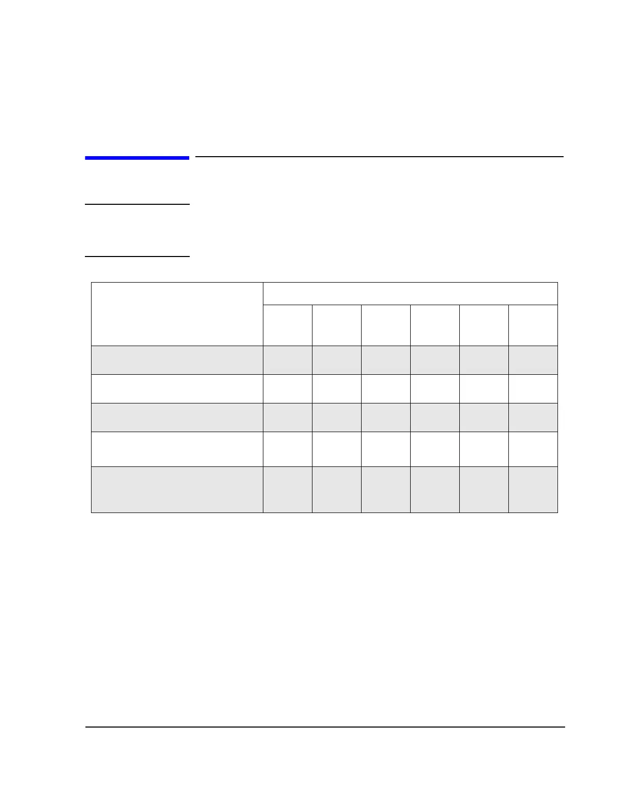
A12 Synthesizer/Doubler Board
A12 Synthesizer/Doubler Board
NOTE: The node voltages given in the following table are approximate values based on a sample
of signal generators. Your signal generator may not reflect these exact values. Additionally,
the resolution of these values varies from node to node. As a guideline, interpret your
measurements based on the number of decimal places shown for the expected voltage.
A12 Synthesizer/Doubler Board Abus Nodes
Test Conditions
Node Voltages (Corrected Values in Vdc)
F2
RF_OUT
TUNE
LOOP
10V
FM
PRESET; FREQUENCY 500.000001 MHz;
No
Modulation
4 0.4 to
0.7
3.0 to 4.8 0.6 9.9 to 10.1 < 0.2
PRESET; FREQUENCY 750 MHz;
No
Modulation
5.5 0.4 to
0.7
10.2 to
12.8
1.5 9.9 to 10.1 < 0.2
PRESET; FREQUENCY 1000 MHz;
No
Modulation
7.2 0.4 to
0.7
17.7 to
23.2
5.5 9.9 to 10.1 < 0.2
+1 Vdc Applied to EXT 1 INPUT:
PRESET; FM On; FM Source Ext 1 DC
2.0
+1 Vdc Applied to EXT 1 INPUT:
PRESET; FREQUENCY < 250 MHz;
FM
On; FM Source Ext 1 DC
2.0
 Loading...