5-14 Service Guide N5230-90014
Theory of Operation PNA Series Microwave Network Analyzers
Synthesized Source Group Operation N5230A
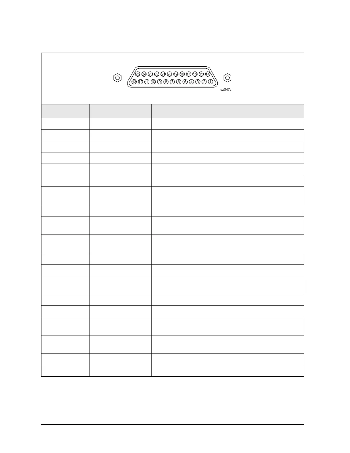
Table 5-5 AUX I/O Connector Pin Assignments
DB-25 Male Connector
Pin Numbers Name Function
1 ACOM 0 V, ground reference for analog signals
2–3 Analog Out 2–1 −10 to +10 Vdc output, 10 mA max, Ro = 100 Ω
4 No connect For future enhancements
5 DCOM 0 V, ground reference for digital signals
6–8 Pulse Out 3–1 TTL out, programmable pulse (for future use)
9 +5 V +5 Vdc output, 100 mA max.
10 Pass/Fail Write
Strobe
TTL out, active low (1 μs min) indicates pass/fail line is
valid
11 Sweep End TTL out, active low (10 μs min) indicates sweep is done
12 Pass/Fail TTL out, latched, indicates pass or fail (programmable
polarity)
13 Output Port Write
Strobe
TTL out, active low (10 μs min) writes I/O port data
14 Analog In −10 to +10 Vdc input, Ri = 100k Ω
15 ACOM 0 V, ground reference for analog signals
16 Power Button In Open-collector input, active low replicates a power
button press
17 DCOM 0 V, ground reference for digital signals
18 Ready for Trigger TTL out, low indicates ready for external trigger
19 External Trigger In TTL in, level trigger (width >1 μs), programmable
polarity
20 Footswitch In TTL in, active low (width >1 μs), triggers a
programmable event
21 +22 V +22 Vdc output, 100 mA max.
22–25 In/Out Port C0–3 TTL I/O, general purpose
 Loading...