59
8126F–AVR–05/12
ATtiny13A
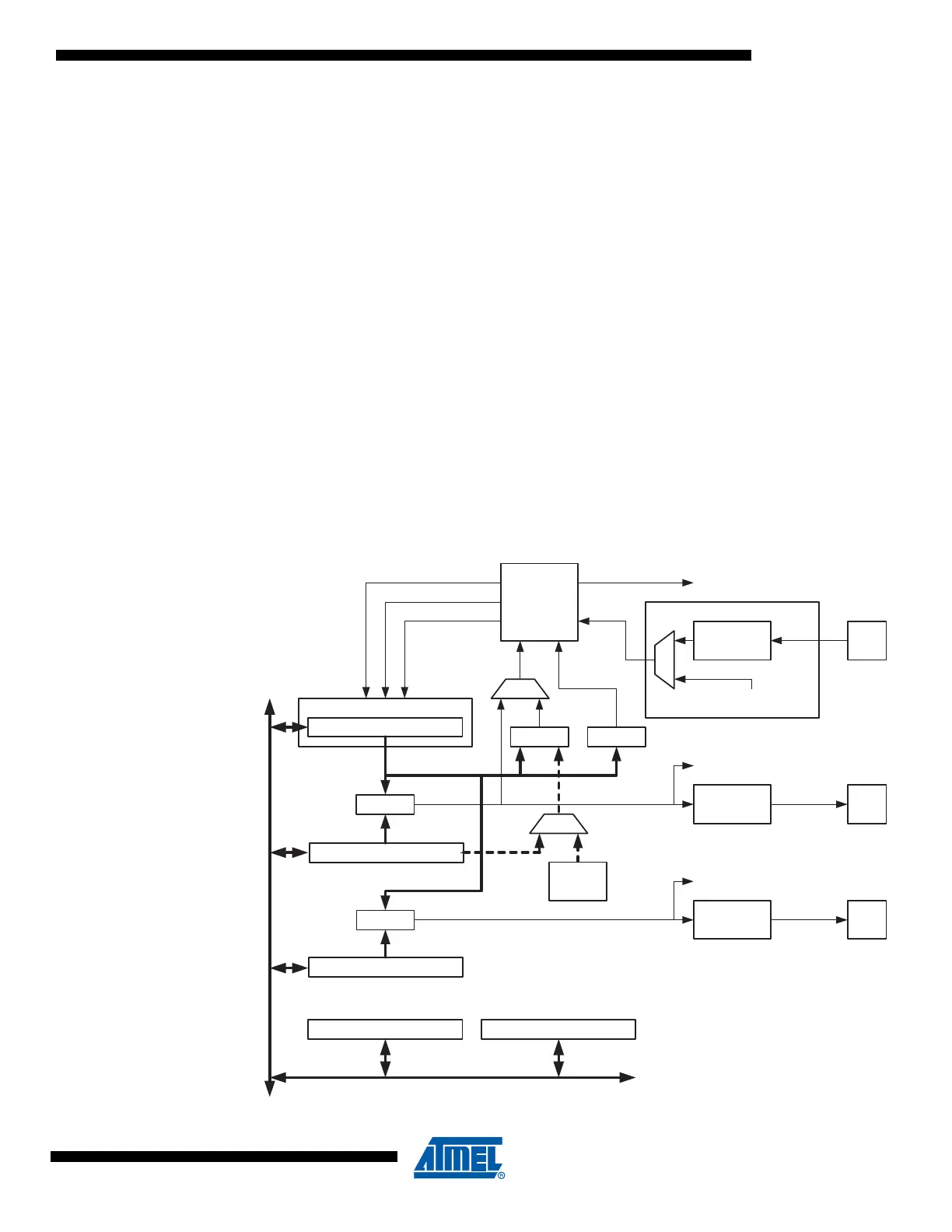
11. 8-bit Timer/Counter0 with PWM
11.1 Features
• Two Independent Output Compare Units
• Double Buffered Output Compare Registers
• Clear Timer on Compare Match (Auto Reload)
• Glitch Free, Phase Correct Pulse Width Modulator (PWM)
• Variable PWM Period
• Frequency Generator
• Three Independent Interrupt Sources (TOV0, OCF0A, and OCF0B)
11.2 Overview
Timer/Counter0 is a general purpose 8-bit Timer/Counter module, with two independent Output
Compare Units, and with PWM support. It allows accurate program execution timing (event man-
agement) and wave generation.
A simplified block diagram of the 8-bit Timer/Counter is shown in Figure 11-1 on page 59. For
the actual placement of I/O pins, refer to “Pinout of ATtiny13A” on page 2. CPU accessible I/O
Registers, including I/O bits and I/O pins, are shown in bold. The device-specific I/O Register
and bit locations are listed in the “Register Description” on page 70.
Figure 11-1. 8-bit Timer/Counter Block Diagram
Clock Select
Timer/Counter
DATA BU S
OCRnA
OCRnB
=
=
TCNTn
Waveform
Generation
Waveform
Generation
OCnA
OCnB
=
Fixed
TOP
Value
Control Logic
= 0
TOP BOTTOM
Count
Clear
Direction
TOVn
(Int.Req.)
OCnA
(Int.Req.)
OCnB
(Int.Req.)
TCCRnA TCCRnB
Tn
Edge
Detector
( From Prescaler )
clk
Tn