70
8126F–AVR–05/12
ATtiny13A
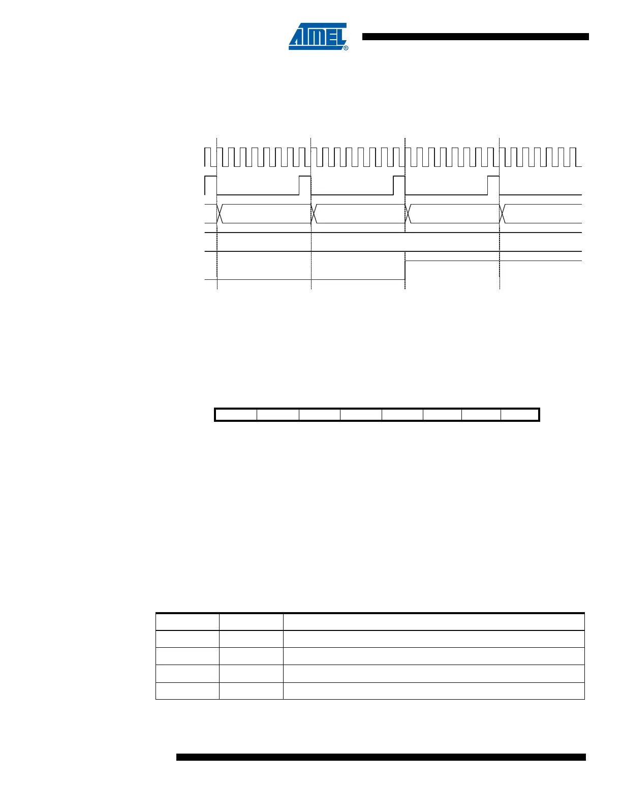
Figure 11-11 shows the setting of OCF0A and the clearing of TCNT0 in CTC mode and fast
PWM mode where OCR0A is TOP.
Figure 11-11. Timer/Counter Timing Diagram, Clear Timer on Compare Match mode, with Pres-
caler (f
clk_I/O
/8)
11.9 Register Description
11.9.1 TCCR0A – Timer/Counter Control Register A
• Bits 7:6 – COM0A[1:0]: Compare Match Output A Mode
These bits control the Output Compare pin (OC0A) behavior. If one or both of the COM0A[1:0]
bits are set, the OC0A output overrides the normal port functionality of the I/O pin it is connected
to. However, note that the Data Direction Register (DDR) bit corresponding to the OC0A pin
must be set in order to enable the output driver.
When OC0A is connected to the pin, the function of the COM0A[1:0] bits depends on the
WGM0[2:0] bit setting.
Table 11-2 shows the COM0A[1:0] bit functionality when the WGM0[2:0] bits are set to a normal
or CTC mode (non-PWM).
OCFnx
OCRnx
TCNTn
(CTC)
TOP
TOP - 1 TOP BOTTOM BOTTOM + 1
clk
I/O
clk
Tn
(clk
I/O
/8)
Bit 7 6 5 4 3210
0x2F COM0A1 COM0A0 COM0B1 COM0B0 – – WGM01 WGM00 TCCR0A
Read/Write R/W R/W R/W R/W R R R/W R/W
Initial Value 0 0 0 0 0 0 0 0
Table 11-2. Compare Output Mode, non-PWM Mode
COM0A1 COM0A0 Description
0 0 Normal port operation, OC0A disconnected.
0 1 Toggle OC0A on Compare Match
1 0 Clear OC0A on Compare Match
1 1 Set OC0A on Compare Match