57
8126F–AVR–05/12
ATtiny13A
10.4 Register Description
10.4.1 MCUCR – MCU Control Register
• Bits 7, 2 – Res: Reserved Bits
These bits are reserved bits in the ATtiny13A and will always read as zero.
• Bit 6 – PUD: Pull-up Disable
When this bit is written to one, the pull-ups in the I/O ports are disabled even if the DDxn and
PORTxn Registers are configured to enable the pull-ups ({DDxn, PORTxn} = 0b01). See “Con-
figuring the Pin” on page 50 for more details about this feature.
10.4.2 PORTB – Port B Data Register
10.4.3 DDRB – Port B Data Direction Register
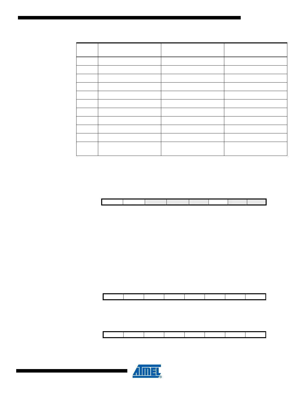
Table 10-5. Overriding Signals for Alternate Functions in PB[2:0]
Signal
Name
PB2/SCK/ADC1/
T0/PCINT2
PB1/MISO/AIN1/
OC0B/INT0/PCINT1
PB0/MOSI/AIN0/
AREF/OC0A/PCINT0
PUOE000
PUOV000
DDOE 0 0 0
DDOV 0 0 0
PVOE 0 OC0B Enable OC0A Enable
PVOV 0 OC0B OC0A
PTOE000
DIEOE PCINT2 • PCIE + ADC1D PCINT1 • PCIE + AIN1D PCINT0 • PCIE + AIN0D
DIEOV ADC1D AIN1D AIN0D
DI T0/PCINT2 Input INT0/PCINT1 Input PCINT0 Input
AIO ADC1 Input
Analog Comparator
Negative Input
Analog Comparator Positive
Input
Bit 7 6 5 4 3 2 1 0
0x35 – PUD
SE SM1 SM0 – ISC01 ISC00 MCUCR
Read/Write R R/W R/W R/W R/W R R/W R/W
Initial Value 0 0 0 0 0 0 0 0
Bit 76543210
0x18 – – PORTB5 PORTB4 PORTB3 PORTB2 PORTB1 PORTB0 PORTB
Read/Write R R R/W R/W R/W R/W R/W R/W
Initial Value 0 0 0 0 0 0 0 0
Bit 76543210
0x17 – – DDB5 DDB4 DDB3 DDB2 DDB1 DDB0 DDRB
Read/Write R R R/W R/W R/W R/W R/W R/W
Initial Value 0 0 0 0 0 0 0 0