16
8126F–AVR–05/12
ATtiny13A
When using register indirect addressing modes with automatic pre-decrement and post-incre-
ment, the address registers X, Y, and Z are decremented or incremented.
The 32 general purpose working registers, 64 I/O Registers, and the 64 bytes of internal data
SRAM in the ATtiny13A are all accessible through all these addressing modes. The Register
File is described in “General Purpose Register File” on page 10.
Figure 5-2. Data Memory Map
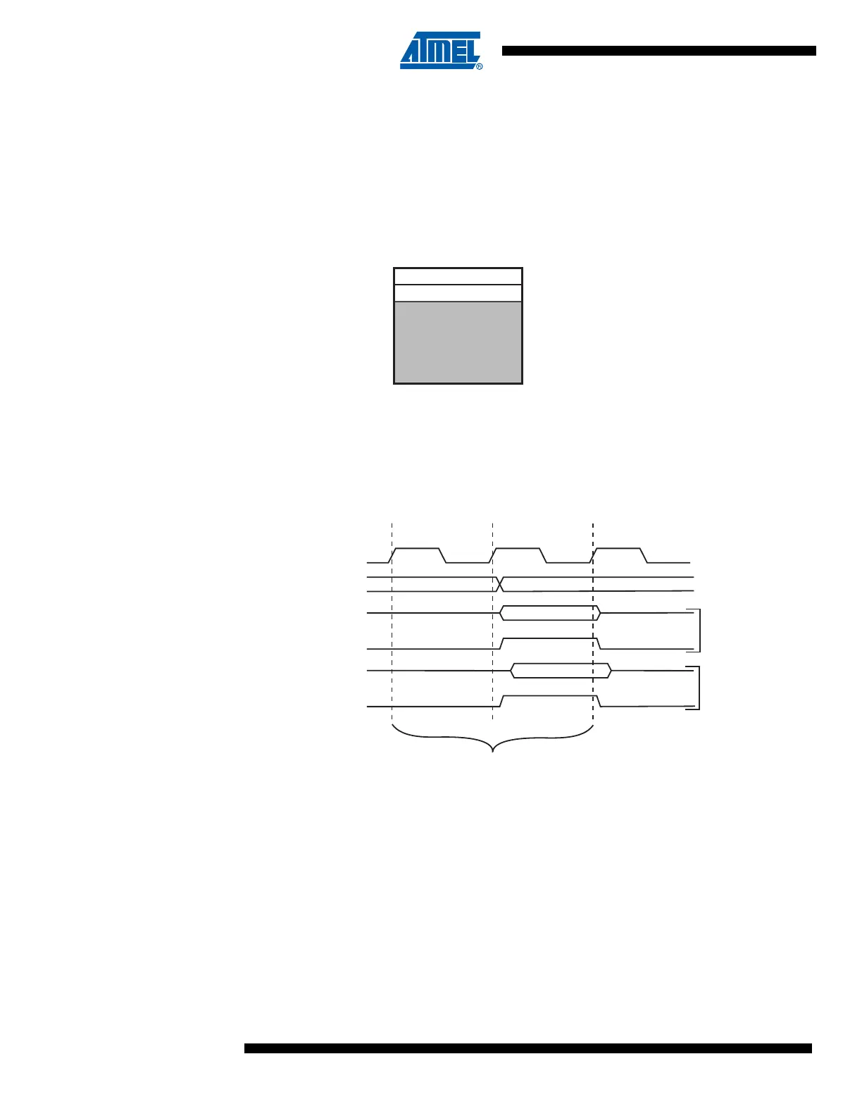
5.2.1 Data Memory Access Times
This section describes the general access timing concepts for internal memory access. The
internal data SRAM access is performed in two clk
CPU
cycles as described in Figure 5-3.
Figure 5-3. On-chip Data SRAM Access Cycles
5.3 EEPROM Data Memory
The ATtiny13A contains 64 bytes of data EEPROM memory. It is organized as a separate data
space, in which single bytes can be read and written. The EEPROM has an endurance of at
least 100,000 write/erase cycles. The access between the EEPROM and the CPU is described
in the following, specifying the EEPROM Address Registers, the EEPROM Data Register, and
the EEPROM Control Register. For a detailed description of Serial data downloading to the
EEPROM, see page 106.
32 Registers
64 I/O Registers
Internal SRAM
(64 x 8)
0x0000 - 0x001F
0x0020 - 0x005F
0x009F
0x0060
Data Memory
clk
WR
RD
Data
Data
Address
Address valid
T1 T2 T3
Compute Address
Read
Write
CPU
Memory Access Instruction
Next Instruction