4.1 Device structure
Device description
5290 / 06/2023 enBENNING PV 1-1+16
4 Device description
4.1
Device structure
1
14
13
9
11
8
15
12
2
4 356
10
77
7
7
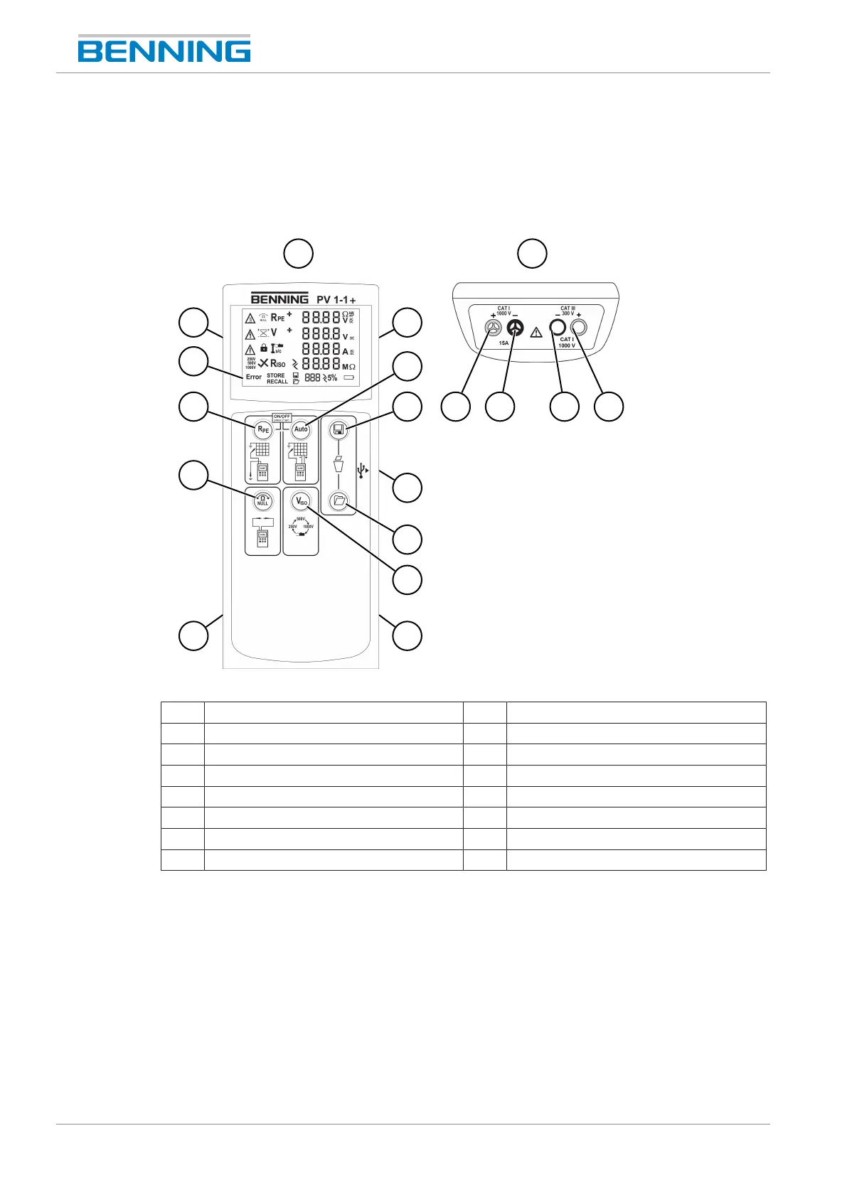
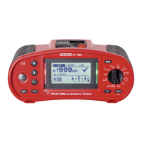
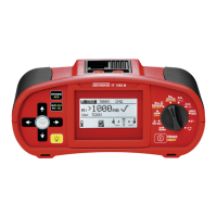
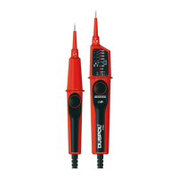
Figure1: BENNING PV 1-1+ device structure
1 Front view of the device 2 Device top
3 Red 4mm test socket “+” 4 Black 4mm test socket “-”
5 Black PV test socket “-” 6 Red PV test socket “+”
7 Bracket für carrying strap 8 “Auto” key
9 “Save” key 10 USB Micro-B interface
11 “Measured value memory” key 12 “V
ISO
” key
13 “NULL balance” key 14 “R
PE
” key
15 Digital display
Rear panel of the device
• Battery compartment
• Notes and information about the device
• Serial number (label, on inside of battery compartment cover)