2
CONTENTS
Safety Information.............................................................................................................................3
Warranty .............................................................................................................................................3
Product Description ..................................................................................................................... 4-7
Specifications................................................................................................................................ 8-9
Electrostatic Discharge Sensitive (ESDS) Device Handling .....................................................10
Part List Notes ................................................................................................................................10
Packaging Part List, FreeSpace
®
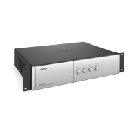
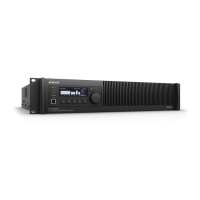
DXA 2120 Amplifier/Mixer (see Figure 1) ............................. 11
Figure 1. FreeSpace DXA 2120 Packaging View ............................................................................ 11
Main Part List, FreeSpace DXA 2120 Amplifier/Mixer (see Figure 2).........................................12
Figure 2. FreeSpace DXA 2120 Amplifier/Mixer Exploded View ......................................................13
Electrical Part Lists .................................................................................................................. 14-52
Control PCB Assembly ............................................................................................................. 14-16
DC24 PCB Assembly ................................................................................................................. 17-18
Digital Signal Processor (DSP) PCB Assembly ..................................................................... 19-28
Input/Output PCB Assembly .................................................................................................... 29-35
Amplifier PCB Assembly ........................................................................................................... 36-40
PSU PCB Assembly................................................................................................................... 41-44
RCA Input PCB Assembly ......................................................................................................... 45-49
RS-232 PCB Assembly ....................................................................................................................50
Speaker PCB Assembly ............................................................................................................ 50-51
Volt PCB Assembly ..........................................................................................................................52
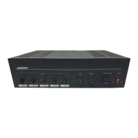
Figure 3. FreeSpace DXA 2120 Amplifier with Top Cover Removed ...............................................53
Disassembly Procedures ......................................................................................................... 54-61
Test Procedures ....................................................................................................................... 62-70
FreeSpace DXA-2120 Firmware Update Procedure .............................................................. 71-72
FreeSpace DXA-2120 Wiring Diagram ..........................................................................................74
Figure 4. DSP and MCU PCB Topside Etch Layout........................................................................75
Figure 5. DSP and MCU PCB Bottom Etch Layout ........................................................................75
Figure 6. Input/Output PCB Topside Etch Layout............................................................................76
Figure 7. Input/Output PCB Bottom Etch Layout ............................................................................76
Figure 8. Volt PCB Topside Etch Layout .........................................................................................77
Figure 9. Volt PCB Bottom Etch Layout ..........................................................................................77
Figure 10. Speaker PCB Topside Etch Layout ................................................................................77
Figure 11. Speaker PCB Bottom Etch Layout .................................................................................77
Figure 12. RS232 PCB Topside Etch Layout ..................................................................................77
Figure 13. RS232 PCB Bottom Etch Layout...................................................................................77
Figure 14. PSU PCB Topside Etch Layout......................................................................................78
Figure 15. PSU PCB Bottom Etch Layout ......................................................................................78
Figure 16. Amplifier PCB Topside Etch Layout................................................................................79
Figure 17. Amplifier PCB Bottom Etch Layout ................................................................................79
Figure 18. DC24 PCB Topside Etch Layout....................................................................................79
Figure 19. DC24 PCB Bottom Etch Layout ....................................................................................79
Figure 20. Control and Display PCB Topside Etch Layout..............................................................80
Figure 21. Control and Display PCB Bottom Etch Layout...............................................................80
Figure 22. RCA Input and A/D PCB Topside Etch Layout................................................................81
Figure 23. RCA Input and A/D PCB Bottom Etch Layout ................................................................81
Integrated Circuit Diagrams .................................................................................................... 82-91
Troubleshooting .............................................................................................................................92
Service Manual Revision History .................................................................................................93