EPSON FX-890/2190 Revision B
Operating Principles Overview 47
2.1.2 Circuit Operation
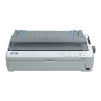
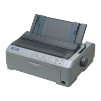
2.1.2.1 C524 MAIN Board
The C524 MAIN board is the control circuit board of this printer. This board consists
of several IC chips and drivers, as described in the table below:
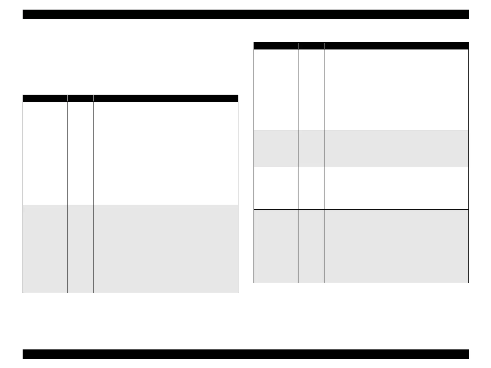
Table 2-2. Major Elements on MAIN Board
Elements Location Function
CPU/ASIC
(2in1ASIC)
IC1
Package: 240 SQFP (0.5 mm between pins)
Manufacturing process: 0.35µ Cell base IC
CPU (H8S/2670 (Hitachi) equivalent)
• Operating frequency: 24 MHz
I/F section (E05B80CC (Hitachi series) equivalent)
• Operating frequency: 48 MHz
• Function: E05B80C
• Memory cycle: 3 states (1 state 41.7 ns, RDNn = 0, no CS
assertion)
Mechanical Controller section (E05B85YA (Fujimi)
equivalent)
• Operating frequency: 24 MHz
• Memory cycle: 3 states (1 state 41.7 ns, RDNn = 0, no CS
assertion)
PROM
(Flash ROM)
IC4
Use: Program
Type: MBM29LV800BA-90
Capacity: 8Mbit
Package: 44SOP
Bit configuration: 8/16 switching type
Bus width: 16 bits
Access time: tCE 181 ns or less
tACC 181 ns or less
tOE 156 ns or less
tDF 60 ns or less
Memory cycle: 3 states 1 weight
(1 state 50.6 ns, RDNn = 0, no CS
assertion)
DRAM IC5
Use: Various buffers, work areas
Device: MSM51V18165D
Type: 2CAS type 16-Mbit DRAM of access time
60 ns with page access function
Bus width: 16 bits
Package: 50-pin TSOP II
Memory cycle: 4 states at normal times (1 state 50.6 ns)
2 states in burst mode (1 state 50.6 ns)
Refresh: Refresh controller of the CPU is used
(CBR method)
Period: 1,024 cycles/16 ms (15.625 us or
less)
EEPROM IC11
Use: Storage of default setting values and
various parameters
Device: S-93C46ADFJ (SII) (10 ms/word writing)
Capacity: 1 kbits
Package: SOP8 pin (150 mil)
Parallel IF circuit
Specification: IEEE1284 compliant Nibble
Data receiving system: Data transfer by DMA
ACK pulse width: Can be selected
Data transfer timing: Can be selected
Transceiver IC: 74LVX161284 (FAIRCHILD) (IC2)
Control circuit: Inside the ASIC
USB IF circuit
Specification: Universal Serial Bus Specification
Revision 1.1
Reception mode:Full speed mode (D+ signal line is pulled
up to +3.3V with 1.5 k
Ω)
Pull-up of D+ signal line is not activated
until the logic system becomes stable after
power on.
Receiving system: Bulk transfer / control transfer
Data reception capacity: About 1.15 MB/s at peak (Bulk
transfer)
Control circuit: Inside the ASIC
Table 2-2. Major Elements on MAIN Board (continued)
Elements Location Function
 Loading...