REV.-A
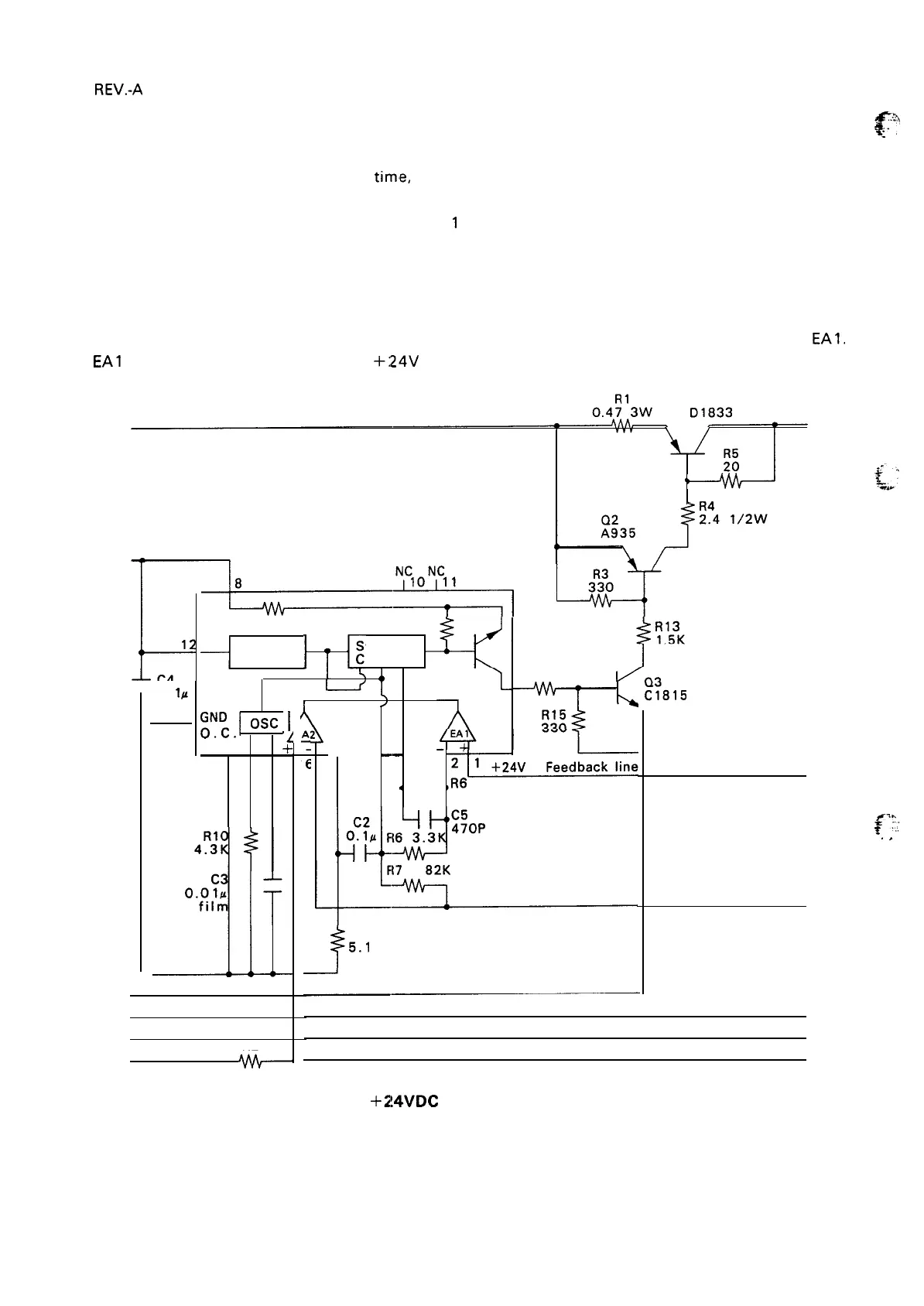
Switching Regulator Circuit
When the voltage is supplied from the rectifying circuit, a 27
KHz switching pulse based on the external
C3-R 10 circuit is created. At the same
time, the standard voltage regulator outputs 5V, which is supplied,
as a comparative voltage, to the negative terminal of error amplifier EA 1. Immediately after power comes
on, + 24V is not yet
being generated, so that EA
1
output will be LOW, and the switching control circuit
will output a switching signal to the base of internal transistor Qx. External transistors Q3, Q2, and Q 1
will operate, and a 36V DC switching
pulse will be output.
The output pulse passes through the smoothing circuit, which converts it to a direct voltage. As
explained below, this voltage is then returned, via a feedback circuit, to the positive terminal of
EA1.
EA1
output is thus controlled so that
+:24V
is always maintained.
L
12
C4
0.
l/A
7
I
I
[<
Switching
Vref
Control
R14
Qx
3.3K
/
GND
O.c.l
osc
I
4
~
—
——
—
13
6
5
5
4 14 3
4
,R6
- 200K
0.1 2W
?
R9
5.1
K
f.
.
.
.
+
,,
.,,
,.
.
2W
f:,
.
.
Figure 2-16.
+I!4VDC
Switching Regulator Circuit
2-14

 Loading...