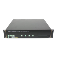
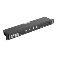
HDSD9545DLY - PRO Profanity Bypass Delay Manual
TECHNICAL DESCRIPTION Revision 1.3.7 Page 4-1
4. TECHNICAL DESCRIPTION
4.1. SPECIFICATIONS
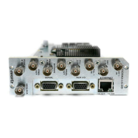
4.1.1. Serial Digital Video Inputs
Standards: SMPTE 292M (1.5 Gb/s), SMPTE 259M (270Mb/s) – see Table 2-3
Number of Inputs: 2
Connector: BNC per IEC 61169-8 Annex A
Equalisation:
HD Video Stds: Automatic up to 50m on Input A and 140m on Input B
with Belden 1694 or equivalent cable
SD Video Stds: Automatic up to 250m with Belden 8281 or equivalent cable
Return Loss:
Input A: > 15 dB up to 1.0 Gb/s, >10dB at 1.5 Gb/s
Input B: > 15 dB up to 1.5 Gb/s
4.1.2. Serial Digital Video Outputs
Standard: Same as Input
Number of Outputs: 5 outputs (2 copies of Output A)
Input A bypass protected to output A1.
Connector: BNC per IEC 61169-8 Annex A
Signal Level: 800mV nominal
DC Offset: 0V ±0.5V
Rise and Fall Time:
HD Video Stds: 200ps nominal
SD Video Stds: 650ps nominal
Overshoot: <10% of amplitude
Wide Band Jitter: < 0.2 UI
Output Return Loss:
A1 > 10 dB up to 1.5 Gb/s
Out A2, B, C, D, E > 15 dB up to 1.5 Gb/s
Output Phase: measured with respect to the Genlock reference
0 to a full frame of offset - separate H and V phase adjustments
4.1.3. Video Reference
Type: Menu selectable - depends on video format (See section Table 2-3)
NTSC or PAL Colour Black 1 V p-p
Composite Bi-level sync (525i/59.94 or 625i/50) 300 mV
HD Tri-level Sync
Connectors: BNC per IEC 61169-8 Annex A
Termination: High impedance loop through or High impedance non-looping or 75 ohm non
looping (jumper selectable)