Reproduction forbidden without Fibocom Wireless Inc. written authorization - All Rights Reserved.
FIBOCOM SU806 Series Hardware Guide Page 36 of 91
VDD_1V8
UART_TXD
UART_CTS
MCU_RTS
0.1uF
UART_RXD
VCCA
OE
VCCB
GND
A1
A2
A3
A4
B4
B3
B2
B1
Level Shifter
0.1uF
VDD_MCU
MCU_TXD
MCU_RXD
MCU_CTS
UART_RTS
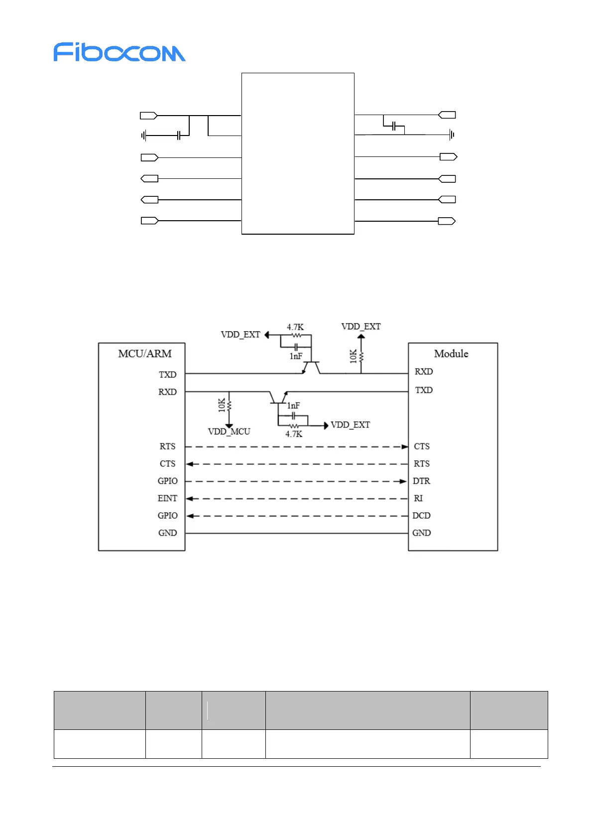
Figure 3-10 Level shift reference design
The other level translator circuit is shown as Figure 3-11, The rest input and output circuit design of dotted
line please refer to solid line part, but pay attention to signal connection direction.
Figure 3-11 Level shift reference design 2
3.5 SPI
SU806 series module provides one master only SPI interface, the pin definition is shown in the following
table:
Table 3-9 SPI pin definition
 Loading...