Reproduction forbidden without Fibocom Wireless Inc. written authorization - All Rights Reserved.
FIBOCOM SU806 Series Hardware Guide Page 39 of 91
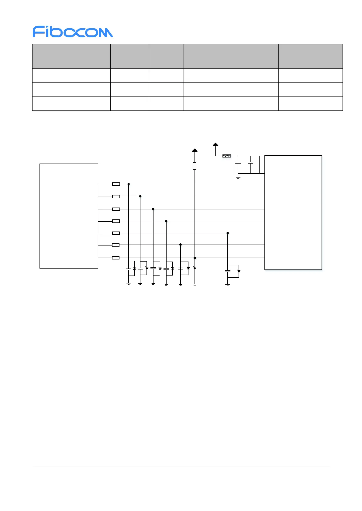
SDIO interface reference design is show in the following figure:
Module
SD_DATA3
SD_DATA1
SD_DATA0
SD_CLK
SD_CMD
DAT3
DAT2
DAT1
DAT0
CLK
CMD
SD_DET
SD_DATA2
22R
22R
22R
22R
22R
22R
DETECTIVE
NC
NC
NC
NC
NC
VDD1V85
4.7uF
100nF
NC
VDDSDCORE
Connector
22R
VDD
100K
100MHz_120R
Figure 3-13 SDIO reference design
SDIO design notice:
1) VDDSDCORE is the SD card peripheral driving power and can provide about 400mA current. SD3.0
need external LDO with power driver ability more than 800mA.
2) Match all SD signals length and pay attention to controlling the width of trace.
3) Pull up SD_DET with VDD1V85.
4) SDIO is a high-speed digital signal cable, needs to be shielded.
3.8 GPIO
SU806 series module have rich GPIOs and the interface level is 1.8V. The pin definition is shown in the
following table:
Table 3-12 GPIO list
 Loading...