Reproduction forbidden without Fibocom Wireless Inc. written authorization - All Rights Reserved.
FIBOCOM SU806 Series Hardware Guide Page 66 of 91
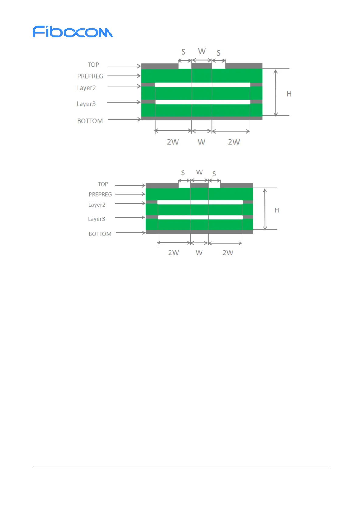
Figure 5-3 Four-layer PCB coplanar waveguide structure (reference ground layer3)
Figure 5-4 Four-layer PCB coplanar waveguide structure (reference ground layer4)
In the design of RF antenna interface circuit, in order to ensure good performance and reliability of the RF
signal, it is recommended to observe the following principles:
The impedance simulation tool should be used to accurately control the RF signal cable at 50Ω
impedance.
The GND pin adjacent to the RF pin should not have thermal welding plate and should be in full
contact with the ground.
The distance between the RF pin and the RF connector should be as short as possible. At the same
time, avoid the right-angle route. The recommended route angle is 135 degrees.
Attention should be paid to the establishment of the component package and the signal pin should be
kept at a certain distance from the ground.
The reference ground plane of the RF signal trace should be entirety; adding a certain amount of
ground holes around the signal and the reference ground can help improve the RF performance; the
distance between the ground hole and the signal trace should be at least 2 times the trace width
(2*W).
 Loading...