GD-Link V2 Adapter User Guide
25
Note: Keep the format of this TXT UTF-8. Please configure programming parameters follow the format
before programming. E.g:
# Program config:
Target CPU: ARM
Program start address: 0x08000000
Erase method: Chip
Reset method: Software
Read protection: Disable
Sram start address: 0x20000000
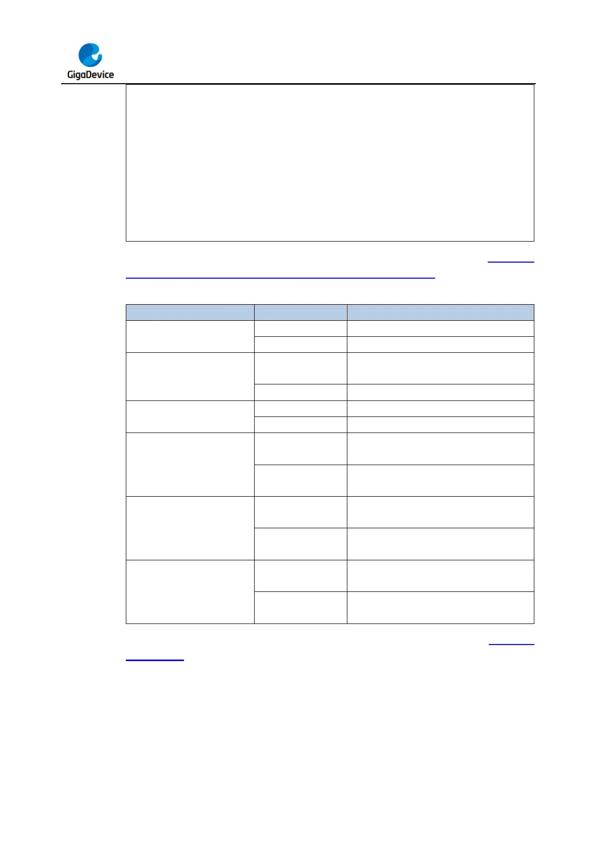
The options and descriptions for each parameter configuration are as shown in Table 3-3.
Drag-and-Drop programming configuration parameter definitions.
Table 3-3. Drag-and-Drop programming configuration parameter definitions
Target MCU core architecture
Select ARM as the target chip core
Select RISC-V as the target chip core
Program flash start address
Program flash start address
Program flash start address 0x0CXXXXXX
Flash erasing method is page erasing
Flash erasing method is full chip erasing
Reset method after completing chip download
is software reset
Reset method after completing chip download
is hardware reset
Target chip's SRAM start address is
0x2XXXXXXX
Target chip's SRAM start address is
0x3XXXXXXX
Select SWD as the download interface(only
for ARM)
Select JTAG as the download interface(only
for RISC-V)
After configuring the programming parameters, save and close the file. Refer to the Hardware
introduction section, connect GD-Link V2 to the target chip via SWD (GD Cortex-M core
MCU) or JTAG interface (GD RISC-V core MCU) correctly, then copy or drag the binary
xxx.bin or executable file xxx.hex generated by the IDE or compiler toolchain to the
recognized GigaDevice disk device. The programmer will automatically identify the target chip
and complete the file programming.
After programming is complete, the virtual USB device will unmount and then remount from
the disk. Once mounting is complete, open the GigaDevice disk. If the disk contains only the