Rev. 1.60 104 August 20, 2019 Rev. 1.60 105 August 20, 2019
BS66F340/BS66F350/BS66F360/BS66F370
Touch A/D Flash MCU with LED Driver
BS66F340/BS66F350/BS66F360/BS66F370
Touch A/D Flash MCU with LED Driver
• IFS Register
Bit 7 6 5 4 3 2 1 0
Name — — IFS5 IFS4 IFS3 IFS2 IFS1 IFS0
R/W — — R/W R/W R/W R/W R/W R/W
POR — — 0 0 0 0 0 0
Bit 7~6 Unimplemented, read as "0"
Bit 5~4 IFS5~IFS4: SCS
input source pin selection
00/10: PA2
01/11: PA3
Bit 3~2 IFS3~IFS2: PTPI input source pin selection
00/10: PB2
01/11: PB4
Bit 1~0 IFS1~IFS0: STPI input source pin selection
00/01: PE2
01/11: PE3
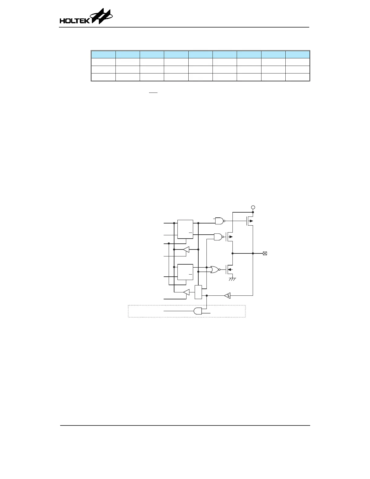
I/O Pin Structures
The accompanying diagrams illustrate the internal structures of some generic I/O pin types. As
the exact logical construction of the I/O pin will differ from these drawings, they are supplied as a
guide only to assist with the functional understanding of the I/O pins. The wide range of pin-shared
structures does not permit all types to be shown.
Generic Input/Output Structure