Rev. 1.60 64 August 20, 2019 Rev. 1.60 65 August 20, 2019
BS66F340/BS66F350/BS66F360/BS66F370
Touch A/D Flash MCU with LED Driver
BS66F340/BS66F350/BS66F360/BS66F370
Touch A/D Flash MCU with LED Driver
• EED Register
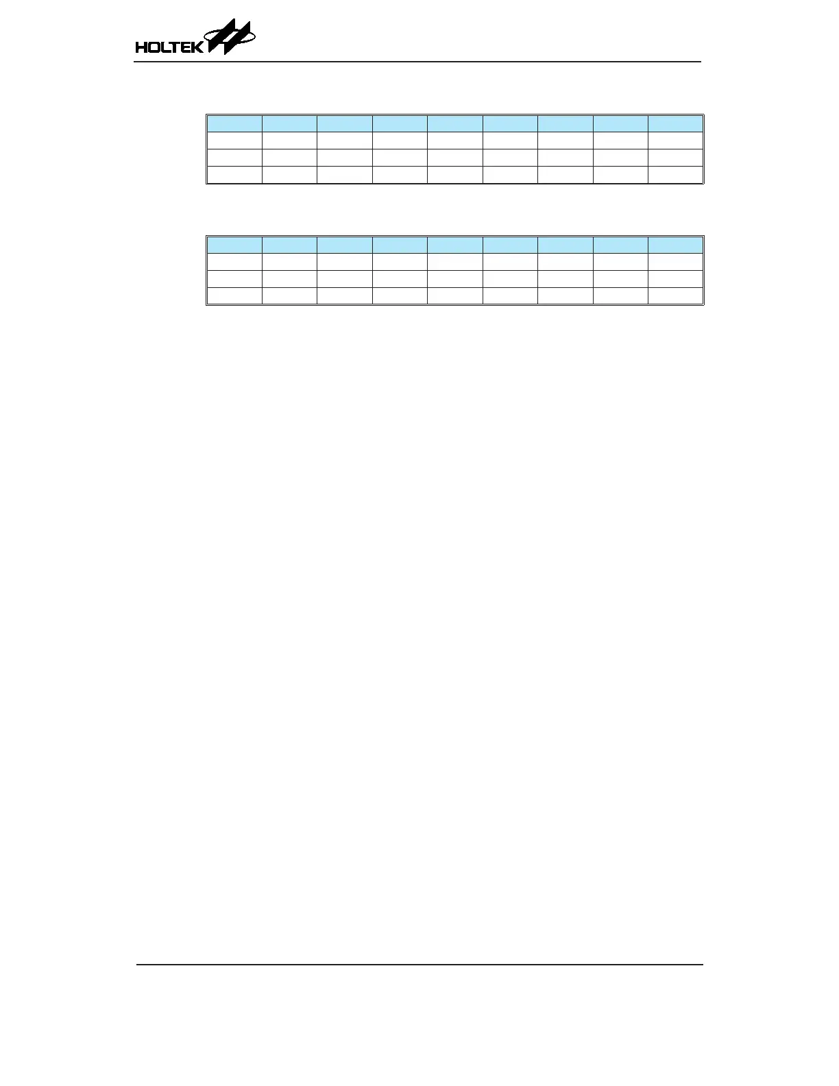
Bit 7 6 5 4 3 2 1 0
Name D7 D6 D5 D4 D3 D2 D1 D0
R/W R/W R/W R/W R/W R/W R/W R/W R/W
POR 0 0 0 0 0 0 0 0
Bit 7~0 D7~D0: Data EEPROM data bit 7~bit0
• EEC Register
Bit 7 6 5 4 3 2 1 0
Name — — — — WREN WR RDEN RD
R/W — — — — R/W R/W R/W R/W
POR — — — — 0 0 0 0
Bit 7~4 Unimplemented, read as "0"
Bit 3 WREN: Data EEPROM write enable
0: Disable
1: Enable
This is the Data EEPROM Write Enable Bit which must be set high before Data
EEPROM write operations are carried out. Clearing this bit to zero will inhibit Data
EEPROM write operations.
Bit 2 WR: EEPROM write control
0: Write cycle has nished
1: Activate a write cycle
This is the Data EEPROM Write Control Bit and when set high by the application
program will activate a write cycle. This bit will be automatically reset to zero by the
hardware after the write cycle has nished. Setting this bit high will have no effect if
the WREN has not rst been set high.
Bit 1 RDEN: Data EEPROM read enable
0: Disable
1: Enable
This is the Data EEPROM Read Enable Bit which must be set high before Data
EEPROM read operations are carried out. Clearing this bit to zero will inhibit Data
EEPROM read operations.
Bit 0 RD: EEPROM read control
0: Read cycle has nished
1: Activate a read cycle
This is the Data EEPROM Read Control Bit and when set high by the application
program will activate a read cycle. This bit will be automatically reset to zero by the
hardware after the read cycle has nished. Setting this bit high will have no effect if
the RDEN has not rst been set high.
Note: The WREN, WR, RDEN and RD can not be set to "1" at the same time in one
instruction. The WR and RD can not be set to "1" at the same time.