Rev. 1.60 150 August 20, 2019 Rev. 1.60 151 August 20, 2019
BS66F340/BS66F350/BS66F360/BS66F370
Touch A/D Flash MCU with LED Driver
BS66F340/BS66F350/BS66F360/BS66F370
Touch A/D Flash MCU with LED Driver
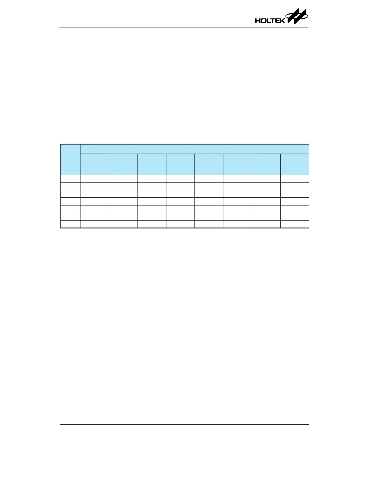
The clock source for the A/D converter, which originates from the system clock f
SYS
, can be chosen
to be either f
SYS
or a subdivided version of f
SYS
. The division ratio value is determined by the
SACKS2~SACKS0 bits in the SADC1 register. Although the A/D clock source is determined by the
system clock f
SYS
and by bits ADCK2~ADCK0, there are some limitations on the maximum A/D
clock source speed that can be selected. As the recommended range of permissible A/D clock period,
t
ADCK
, is from 0.5μs to 10μs, care must be taken for system clock frequencies. For example, as the
system clock operates at a frequency of 8MHz, the ADCK2~ADCK0 bits should not be set to 000,
001 or 111. Doing so will give A/D clock periods that are less than the minimum A/D clock period
which may result in inaccurate A/D conversion values. Refer to the following table for examples,
where values marked with an asterisk * show where, depending upon the device, special care must
be taken, as the values may be less than the specied minimum A/D Clock Period.
However, the recommended A/D clock period is from 1μs to 2μs if the input signal to be converted
is the temperature sensor output voltage or reference voltage.
f
SYS
A/D Clock Period (t
ADCK
)
ADCK[2:0]
= 000
(f
SYS
)
ADCK[2:0]
= 001
(f
SYS
/2)
ADCK[2:0]
= 010
(f
SYS
/4)
ADCK[2:0]
= 011
(f
SYS
/8)
ADCK[2:0]
= 100
(f
SYS
/16)
ADCK[2:0]
= 101
(f
SYS
/32)
ADCK[2:0]
= 110
(f
SYS
/64)
ADCK[2:0]
= 111
(f
SYS
/128)
1 MHz 1μs 2μs 4μs 8μs 16μs * 32μs * 64μs * 128μs *
2 MHz 500ns 1μs 2μs 4μs 8μs 16μs * 32μs * 64μs *
4 MHz 250ns * 500ns 1μs 2μs 4μs 8μs 16μs * 32μs *
8 MHz 125ns * 250ns * 500ns 1μs 2μs 4μs 8μs 16μs *
12 MHz 83ns * 167ns * 333ns * 667ns 1.33μs 2.67μs 5.33μs 10.67μs *
16 MHz 62.5ns * 125ns * 250ns * 500ns 1μs 2μs 4μs 8μs
20 MHz 50ns * 100ns * 200ns * 400ns * 800ns 1.6μs 3.2μs 6.4μs
A/D Clock Period Examples for External Analog Inputs
However, the recommended A/D clock period is from 1μs to 2μs if the input signal to be converted
is the temperature sensor output voltage or reference voltage.
Controlling the power on/off function of the A/D converter circuitry is implemented using the
ADCEN bit in the ADCR0 register. This bit must be set high to power on the A/D converter.
When the ADCEN bit is set high to power on the A/D converter internal circuitry a certain delay,
as indicated in the timing diagram, must be allowed before an A/D conversion is initiated. Even if
no pins are selected for use as A/D inputs, if the ADCEN bit is high, then some power will still be
consumed. In power conscious applications it is therefore recommended that the ADCEN is set low
to reduce power consumption when the A/D converter function is not being used.
A/D Converter Reference Voltage
The reference voltage supply to the A/D Converter can be supplied from the positive power supply
pin, V
DD
, an external reference source supplied on pin VREF or an internal temperature sensor
reference voltage V
TSVREF
. The internal temperature sensor reference voltage can be derived from the
intenal V
BG
or V
PTAT
voltage selected using the K_VPTAT bit in the TSC3 register and then amplied
through a programmable gain amplifier except the one sourced from V
DD
. The PGA gain can be
equal to 1.675 or 1 selected by the K_REFO bit in the TSC0 register. As the VREF pin is pin-shared
with other functions, when the VREF pin is selected as the reference voltage supply pin, the VREF
pin-shared function control bits should first be properly configured to disable other pin-shared
functions.