Rev. 1.60 144 August 20, 2019 Rev. 1.60 145 August 20, 2019
BS66F340/BS66F350/BS66F360/BS66F370
Touch A/D Flash MCU with LED Driver
BS66F340/BS66F350/BS66F360/BS66F370
Touch A/D Flash MCU with LED Driver
Analog to Digital Converter
The need to interface to real world analog signals is a common requirement for many electronic
systems. However, to properly process these signals by a microcontroller, they must first be
converted into digital signals by A/D converters. By integrating the A/D conversion electronic
circuitry into the microcontroller, the need for external components is reduced signicantly with the
corresponding follow-on benets of lower costs and reduced component space requirements.
A/D Converter Overview
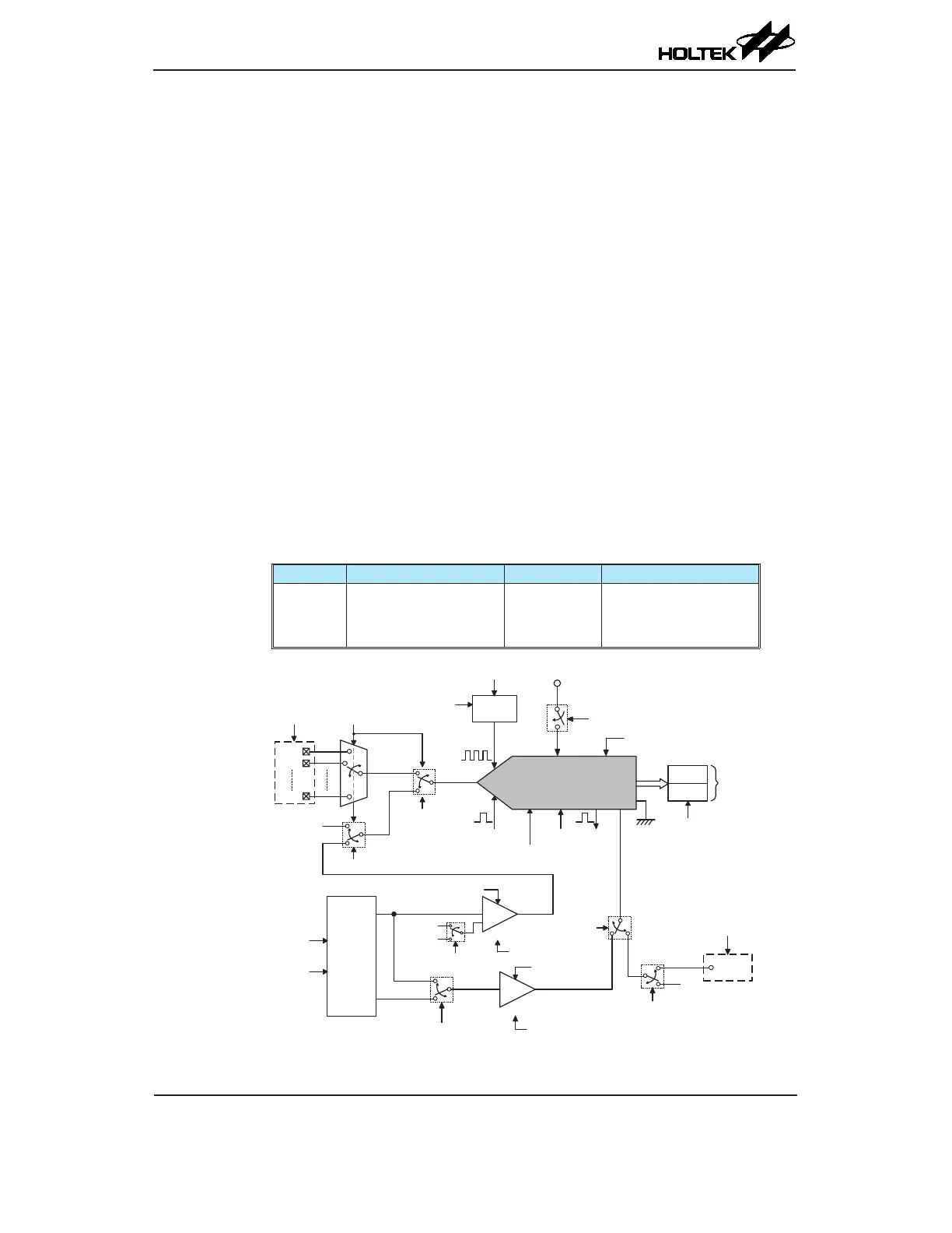
These devices contain a multi-channel analog to digital converter which can directly interface to
external analog signals, such as that from sensors or other control signals and convert these signals
directly into a 12-bit digital value. It also can convert the internal signals, such as the Temperature
semsor output or Temperature sensor reference voltage, into a 12-bit digital value. The external or
internal analog signal to be converted is determined by the ACS3~ACS0 bits together with the TSE
and BGMEN bits. When the external analog signal is to be converted, the corresponding pin-shared
control bits should rst be properly congured and then desired external channel input should be
selected using the ACS3~ACS0 bits.
This A/D converter also includes a temperature sensor circuitry which contains a temperature
sensor, operational ampliers and an internal reference voltage. The temperature sensor will detect
the temperature and output a voltage proportional to the temperature. The output voltage can be
amplied by the OPA and then converted to an 12-bit digital data using the A/D converter.
The accompanying block diagram shows the internal structure of the A/D converter with temperature
sensor together with its associated registers and control bits.
Device External Input Channels Internal Signal A/D Channel Select Bits
BS66F340
BS66F350
BS66F360
BS66F370
8: AN0~AN7 2: V
TSO
, V
TSVREF
ACS3~ACS0
TSE, BGMEN
Pin-shared
Selection
ACS3~ACS0
A/D Converter
START
ADBZ
V
SS
A/D Clock
÷2
N
(N=0~7)
f
SYS
ADCK2~ADCK0
V
DD
ADCEN
ADRL
ADRH
AN0
AN1
AN7
A/D Converter
Reference Voltage
A/D Data
ADRFS
VREF
Pin-shared
Selection
IDLE_CONV
ATM
Temp.
Sensor
TSE
BGMEN
V
BGTS
V
PTAT
OPA1
Gain=1.675 or 1
K_VPTAT
OP1EN
K_REFO
OPA2
OP2EN
Gain=4 or 5
G5XEN
V
TSO
V
DD
TSE
BGMEN
V
TSVREF
VREFP_EXT
1xxxB
V
TSO
V
TSVREF
V
PTAT
TSCLK_S1~TSCLK_S0
VREFS
V
TSVRI
BIAS
V
TSVREF
V
DD
A/D Converter with Temperature Sensor Diagram