Rev. 1.60 210 August 20, 2019 Rev. 1.60 211 August 20, 2019
BS66F340/BS66F350/BS66F360/BS66F370
Touch A/D Flash MCU with LED Driver
BS66F340/BS66F350/BS66F360/BS66F370
Touch A/D Flash MCU with LED Driver
Time Base Interrupt
The function of the Time Base Interrupt is to provide regular time signal in the form of an internal
interrupt. It is controlled by the overflow signal from its internal timer. When this happens its
interrupt request ag, TBnF, will be set. To allow the program to branch to its respective interrupt
vector addresses, the global interrupt enable bit, EMI and Time Base enable bit, TBnE, must rst be
set. When the interrupt is enabled, the stack is not full and the Time Base overows, a subroutine
call to its respective vector location will take place. When the interrupt is serviced, the interrupt
request flag, TBnF, will be automatically reset and the EMI bit will be cleared to disable other
interrupts.
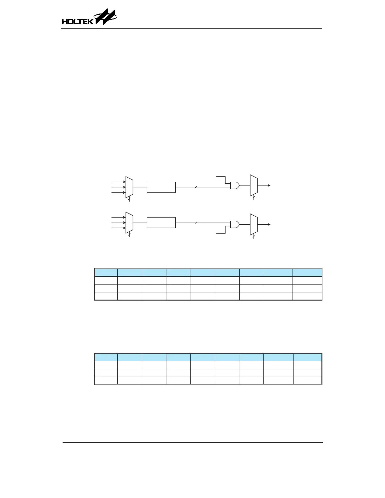
The purpose of the Time Base Interrupt is to provide an interrupt signal at xed time periods. Its
clock source, f
PSC0
or f
PSC1
, originates from the internal clock source f
SYS
, f
SYS
/4 or f
SUB
and then
passes through a divider, the division ratio of which is selected by programming the appropriate bits
in the TB0C and TB1C registers to obtain longer interrupt periods whose value ranges. The clock
source which in turn controls the Time Base interrupt period is selected using the CLKSEL0[1:0]
and CLKSEL1[1:0] bits in the PSCR0 and PSCR1 register respectively.
M
U
X
f
SYS
/4
f
SYS
f
SUB
Prescaler 0
CLKSEL0[1:0]
f
PSC0
f
PSC0
/2
8
~ f
PSC0
/2
15
M
U
X
M
U
X
TB0[2:0]
TB1[2:0]
Time Base 0 Interrupt
Time Base 1 Interrupt
TB0ON
TB1ON
M
U
X
f
SYS
/4
f
SYS
f
SUB
Prescaler 1
CLKSEL1[1:0]
f
PSC1
f
PSC1
/2
8
~ f
PSC1
/2
15
Time Base Interrupts
• PSCR0 Register
Bit 7 6 5 4 3 2 1 0
Name — — — — — — CLKSEL01 CLKSEL00
R/W — — — — — — R/W R/W
POR — — — — — — 0 0
Bit 7~2 unimplemented, read as "0"
Bit 1~0 CLKSEL01~CLKSEL00: Prescaler 0 clock source selection
00: f
SYS
01: f
SYS
/4
1x: f
SUB
• PSCR1 Register
Bit 7 6 5 4 3 2 1 0
Name — — — — — — CLKSEL11 CLKSEL10
R/W — — — — — — R/W R/W
POR — — — — — — 0 0
Bit 7~2 unimplemented, read as "0"
Bit 1~0 CLKSEL11~CLKSEL10: Prescaler 1 clock source selection
00: f
SYS
01: f
SYS
/4
1x: f
SUB