Rev. 1.60 156 August 20, 2019 Rev. 1.60 157 August 20, 2019
BS66F340/BS66F350/BS66F360/BS66F370
Touch A/D Flash MCU with LED Driver
BS66F340/BS66F350/BS66F360/BS66F370
Touch A/D Flash MCU with LED Driver
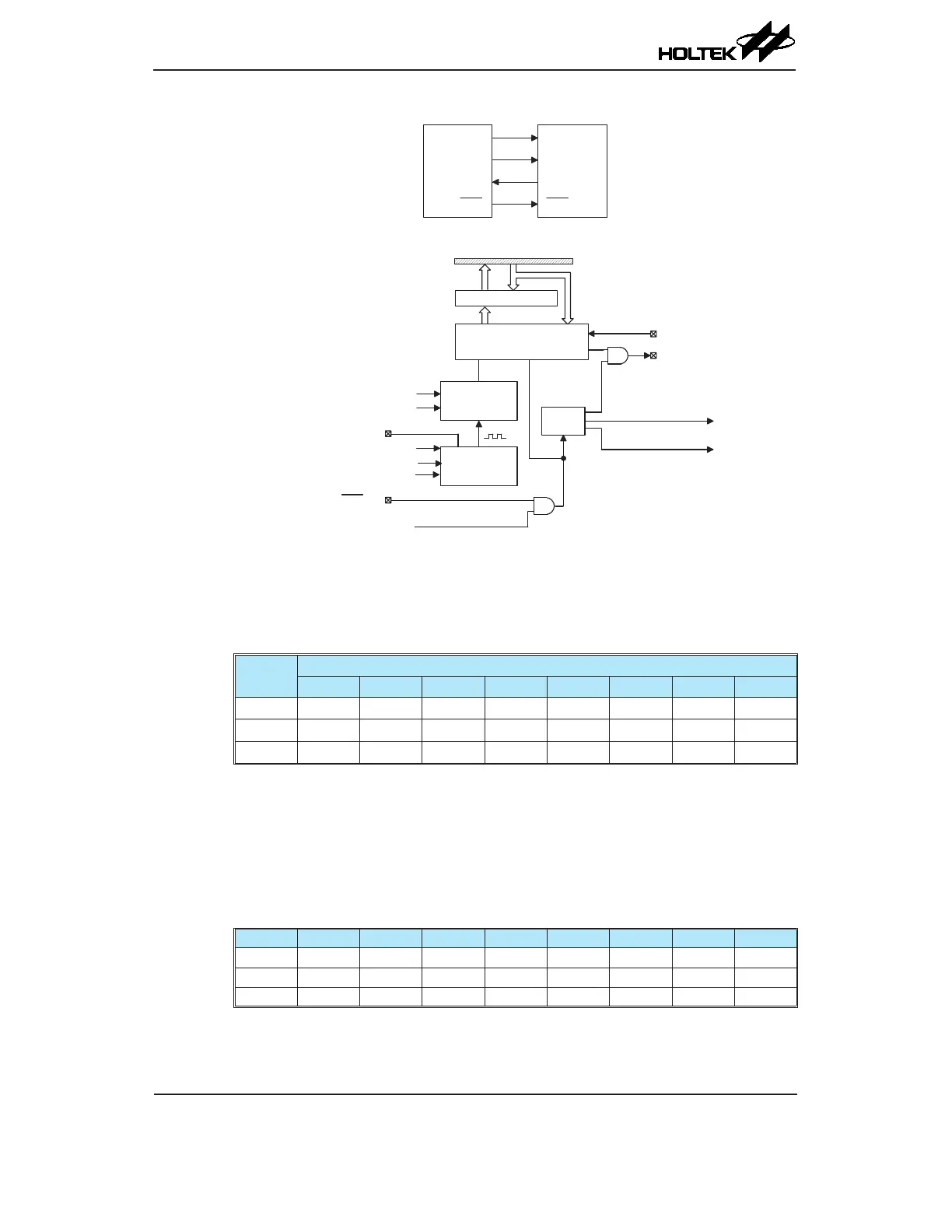
SPI Master/Slave Connection
SPI Block Diagram
SPI Registers
There are three internal registers which control the overall operation of the SPI interface. These are
the SIMD data register and two registers SIMC0 and SIMC2. Note that the SIMC1 register is only
used by the I
2
C interface.
Register
Name
Bit
7 6 5 4 3 2 1 0
SIMC0 SIM2 SIM1 SIM0 — SIMDEB1 SIMDEB0 SIMEN SIMICF
SIMC2 D7 D6 CKPOLB CKEG MLS CSEN WCOL TRF
SIMD D7 D6 D5 D4 D3 D2 D1 D0
SPI Registers List
• SIMD Register
The SIMD register is used to store the data being transmitted and received. The same register is used
by both the SPI and I
2
C functions. Before the device writes data to the SPI bus, the actual data to
be transmitted must be placed in the SIMD register. After the data is received from the SPI bus, the
device can read it from the SIMD register. Any transmission or reception of data from the SPI bus
must be made via the SIMD register.
Bit 7 6 5 4 3 2 1 0
Name D7 D6 D5 D4 D3 D2 D1 D0
R/W R/W R/W R/W R/W R/W R/W R/W R/W
POR x x x x x x x x
"x": unknown