Rev. 1.60 42 August 20, 2019 Rev. 1.60 43 August 20, 2019
BS66F340/BS66F350/BS66F360/BS66F370
Touch A/D Flash MCU with LED Driver
BS66F340/BS66F350/BS66F360/BS66F370
Touch A/D Flash MCU with LED Driver
In Application Programming Control Registers
The Address register, FARL and FARH, the Data registers, FD0L/FD0H, FD1L/FD1H, FD2L/FD2H
and FD3L/FD3H, and the Control registers, FC0, FC1 and FC2, are the corresponding Flash access
registers located in Data Memory sector 0 for IAP. If using the indirect addressing method to access
the FC0, FC1 and FC2 registers, all read and write operations to the registers must be performed
using the Indirect Addressing Register, IAR1 or IAR2, and the Memory Pointer pair, MP1L/MP1H
or MP2L/MP2H. Because the FC0, FC1 and FC2 control registers are located at the address of
50H~52H in Data Memory sector 0, the desired value ranged from 50H to 52H must rst be written
into the MP1L or MP2L Memory Pointer low byte and the value "00H" must also be written into the
MP1H or MP2H Memory Pointer high byte.
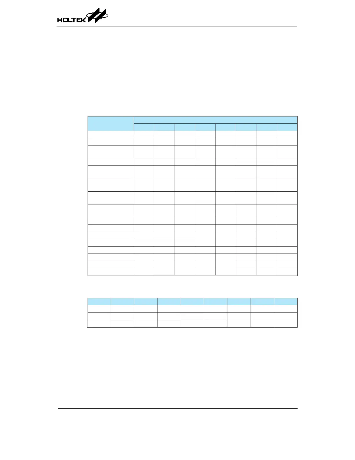
Register
Name
Bit
7 6 5 4 3 2 1 0
FC0 CFWEN FMOD2 FMOD1 FMOD0 FWPEN FWT FRDEN FRD
FC1 D7 D6 D5 D4 D3 D2 D1 D0
FC2
(BS66F350/360/370)
— — — — — — — CLWB
FARL A7 A6 A5 A4 A3 A2 A1 A0
FARH
(BS66F340)
— — — — A11 A10 A9 A8
FARH
(BS66F350)
— — — A12 A11 A10 A9 A8
FARH
(BS66F360)
— — A13 A12 A11 A10 A9 A8
FARH
(BS66F370)
— A14 A13 A12 A11 A10 A9 A8
FD0L D7 D6 D5 D4 D3 D2 D1 D0
FD0H D15 D14 D13 D12 D11 D10 D9 D8
FD1L D7 D6 D5 D4 D3 D2 D1 D0
FD1H D15 D14 D13 D12 D11 D10 D9 D8
FD2L D7 D6 D5 D4 D3 D2 D1 D0
FD2H D15 D14 D13 D12 D11 D10 D9 D8
FD3L D7 D6 D5 D4 D3 D2 D1 D0
FD3H D15 D14 D13 D12 D11 D10 D9 D8
IAP Registers List
• FC0 Register
Bit 7 6 5 4 3 2 1 0
Name CFWEN FMOD2 FMOD1 FMOD0 FWPEN FWT FRDEN FRD
R/W R/W R/W R/W R/W R/W R/W R/W R/W
POR 0 1 1 1 0 0 0 0
Bit 7 CFWEN: Flash Memory Write enable control
0: Flash memory write function is disabled
1: Flash memory write function has been successfully enabled
When this bit is cleared to 0 by application program, the Flash memory write function
is disabled. Note that writing a "1" into this bit results in no action. This bit is used
to indicate that the Flash memory write function status. When this bit is set to 1 by
hardware, it means that the Flash memory write function is enabled successfully.
Otherwise, the Flash memory write function is disabled as the bit content is zero.
 Loading...