Section VI
Communication Information Adapter (ACIA) U13,
and
2
multiplexers U12
and
U27. See Figure
6-2
and
6-24.
6-9.
DATA
INPUT
AND
OUTPUT
CIRCUITS.
Be-
cause
signals
within
the
7475A are positive-true TTL
levels,
inverting
line drivers
and
receivers, U9,
Ull,
and
U26,
are
used to convert
the
logic
and
voltage between
the
levels required
by
the
interface system (shown
in
Table
6-1)
and
the
internal levels. Figure
6-2
is a
diagram
of
the
1/0
circuits
and
the
ACIA.
6-10.
ACIA. The logic level on the Read/Write input
con-
trols
the
direction of
data
flow through
the
data
bus
interface. When
the
RS
(Register Select)
input
is high,
the
R/W
input
selects either
the
receive or
transmit
data
register. When RS
is
low,
the
control/status
registers are
selected.
The
1 MHz
signal
at
the
E
input
clocks
data
in
and
out of
the
ACIA on
the
data
bus
(DO-D7)
and
the
RX/TX clock (Baud Rate Clock) clocks
data
in
and
out
on
the
RXD (Received Data)
and
TXD (Transmitted
Data) lines,
6-11.
MULTIPLEXER Ul2. When the address line
(EIOO)
is
high,
the
7475A
transmitted
data
goes out on
the
Transmitted
Data
line (pin
2).
The Secondary Transmitted
Data
line (pin
14)
is held
at
a negative voltage. When
EIOO
is
low, information on
the
Secondary Received
Data
line
is
retransmitted on
the
Transmitted
Data
line
(pin
2),
and
the
7475A
transmitted
data
goes out on
the
Secondary Transmitted
Data
line (pin
14).
6-12.
MULTIPLEXER
U27.
When the address line (EI03)
is low
and
chip select (CS) from U6, gate
array
B,
is low,
three control lines are passed onto
the
data
bus.
The
functions of these control lines are
as
follows:
a. DATA
SET
READY (DSR) - Activated
by
the
modem
to
tell
the
plotter
that
the
modem
is
operational.
b. CLEAR TO
SEND
(CTS) - Activated
by
the
modem to tell
the
plotter
that
it
is
ready
to receive
and
re-transmit
data
from
the
terminal.
c.
DATA TERMINAL READY (DTR) - Activated
by
the
plotter to tell
the
modem
that
the
terminal
is operational.
6-13.
BAUD RATE.
The
internal
baud
rate
(transmit/
receive) clock
signal
is
derived
in
U5, Gate
Array
A,
from
the
4 MHz clock signal.
The
baud
rate
clock
fre-
quency is sixteen times
the
desired
baud
rate.
Baud
rate
Model 7475A
may
be
selected by
means
of
the
rear-panel switches,
or
an
external clock signal
may
be used.
6-14.
HP-IB INTERFACE (Option
002)
6-15.
HP-IB interface connections
are
shown
on
the
schematic
diagram
at
the
end
of
this
section.
Input/
Output voltage levels
must
meet TTL requirements (low
=
-0.8
V;
high=
-2.0
V).
All
signals
are
active low
(true). Figure
6-3
is
a block
diagram
of
the
HP-IB Inter-
face Circuits.
6-16.
All
data
and
control signals to
and
from
the
HP-IB
go
through
UlO
and
Ull,
the
bus transceivers, which
are enabled to
transmit
or to receive
by
U12,
the
inter-
face
adapter
in
response to HP-IB commands.
The
inter-
face
adapter
automatically
handles
all
handshake
requirements on
the
HP-IB. When
the
plotter power is
on,
the
bus transceiver
inputs
are
high
impedance to
prevent loading
the
data
lines. When
the
plotter power
is
off,
the
bus transceivers present
an
open circuit
to
all
data
lines; consequently,
the
plotter does
not
interfere
with other HP-IB operations.
6-17.
A
16
line bus is used to
carry
data
and
control
information
and
is divided into three sets of lines.
a.
Data
bus - 8
signal
lines -
DIOl
through
DI08.
b.
Data
transfer
control
- 3
signal
lines
(Handshake).
c.
Interface
management
- 5 signal lines.
6-18.
The
data
bus
transfers
8-bit
data
or control words
between
the
controller
and
the
plotter.
The
words are
in
bit parallel byte serial form.
The
words
are
transferred
bi-directionally
and
asynchronously.
6-19.
The three
data
transfer
control lines, or
"hand-
shake
lines"
are
used to control
the
transfer
of informa-
tion on
the
data
bus. These lines are identified
as
follows:
a. DATA VALID
(DAV)-
Used to indicate
that
valid
information
is
available on
the
data
lines.
b. NOT READY FOR DATA (NRFD) - Used to
indicate
the
readiness of
the
Plotter
to accept
information.
c.
Nm'
DATA ACCEfYI'ED (NDAC) - Used to indi-
cate
the
acceptance of information by
the
Plotter.
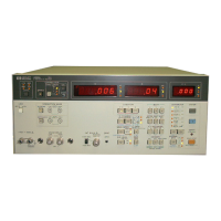
Table
6-1.
RS-232-C/CCI'IT
V.24
Interface Signal Levels
INTERCHANGE VOLTAGE
NOTATION
NEGATIVE POSITIVE
(More Negative
than
-3
V)
(More Positive
than
+3
V)
Binary
State
1 0
Signal Condition
Marking Spacing
Function
off
on
6-2