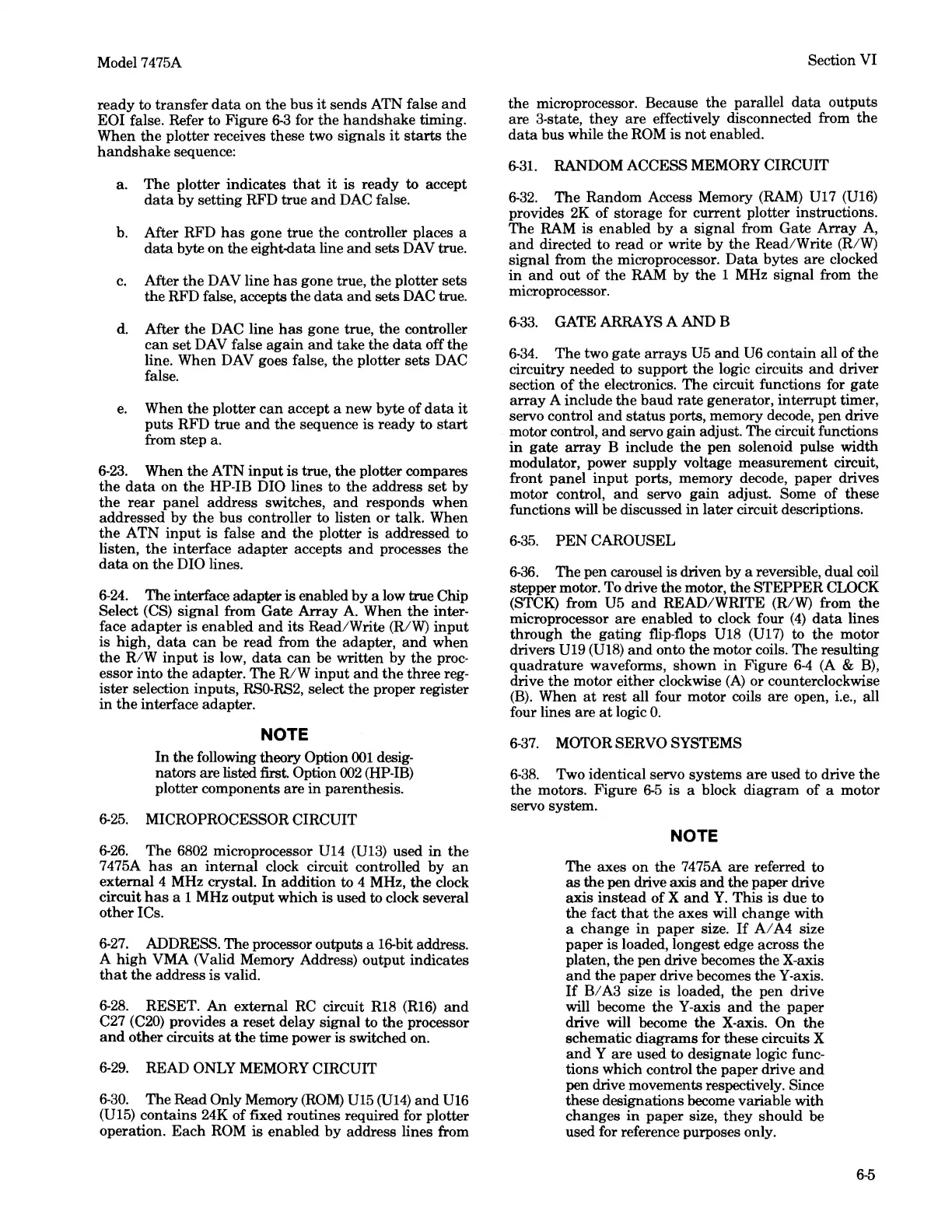
Model 7475A
ready to
transfer
data
on the bus
it
sends ATN false
and
EOI false. Refer to Figure
6-3
for the
handshake
timing.
When the plotter receives these two signals
it
starts
the
handshake
sequence:
a.
The
plotter indicates
that
it
is
ready to accept
data
by
setting RFD true
and
DAC false.
b.
After RFD
has
gone true the controller places a
data
byte on the eight-data line
and
sets
DAV
true.
c.
After
the
DAV line
has
gone true,
the
plotter sets
the RFD false, accepts
the
data
and
sets DAC true.
d.
After
the
DAC line
has
gone true,
the
controller
can
set DAV false
again
and
take the
data
off the
line. When DAV goes false,
the
plotter sets DAC
false.
e.
When
the
plotter
can
accept a new byte
of
data
it
puts
RFD true
and
the
sequence
is
ready to
start
from step a.
6-23.
When
the
ATN
input
is
true,
the
plotter compares
the
data
on
the
HP-IB DIO lines to
the
address
set
by
the
rear
panel address switches,
and
responds
when
addressed
by
the
bus controller to listen
or
talk. When
the
ATN
input
is
false
and
the
plotter
is
addressed to
listen,
the
interface
adapter
accepts
and
processes
the
data
on
the
DIO lines.
6-24.
The interface adapter is enabled
by
a low true Chip
Select (CS)
signal
from Gate
Array
A. When
the
inter-
face
adapter
is
enabled
and
its
Read/Write (R/W)
input
is
high,
data
can
be read from
the
adapter,
and
when
the
R/W
input
is
low,
data
can
be written
by
the
proc-
essor into
the
adapter. The
R/W
input
and
the
three reg-
ister selection inputs,
RSO-RS2,
select the proper register
in
the
interface adapter.
NOTE
In
the
following theory Option
001
desig-
nators are listed first. Option
002
(HP-IB)
plotter components are
in
parenthesis.
6-25.
MICROPROCESSOR CIRCUIT
6-26.
The 6802 microprocessor U14 (U13) used
in
the
7475A
has
an
internal
clock circuit controlled
by
an
external 4 MHz crystal.
In
addition to 4 MHz,
the
clock
circuit
has
a 1 MHz output which
is
used to clock several
otherICs.
6-27.
ADDRESS. The processor outputs a 16-bit address.
A
high
VMA (Valid Memory Address) output indicates
that
the
address
is
valid.
6-28.
RESET.
An
external RC circuit R18
(R16)
and
C27 (C20) provides a reset delay
signal
to
the
processor
and
other circuits
at
the
time power is switched on.
6-29.
READ ONLY MEMORY CIRCUIT
6-30.
The Read Only Memory
(ROM)
U15
(U14)
and
U16
(U15) contains 24K
of
fixed routines required for plotter
operation.
Each
ROM
is
enabled
by
address lines from
Section VI
the microprocessor. Because the parallel
data
outputs
are 3-state, they are effectively disconnected from the
data
bus while the ROM is not enabled.
6-31.
RANDOM ACCESS MEMORY CIRCUIT
6-32.
The Random Access Memory (RAM)
Ul
7 (U16)
provides
2K
of storage for current plotter instructions.
The RAM is enabled
by
a signal from Gate
Array
A,
and
directed to read or write
by
the
Read/Write (R/W)
signal from
the
microprocessor.
Data
bytes are clocked
in
and
out of the RAM by the 1 MHz signal from the
microprocessor.
6-33.
GATE ARRAYS A AND B
6-34.
The two gate
arrays
U5
and
U6 contain all of
the
circuitry needed to support the logic circuits
and
driver
section
of
the
electronics.
The
circuit functions for
gate
array
A include
the
baud
rate
generator, interrupt timer,
servo control
and
status
port.s, memory decode, pen drive
motor control,
and
servo
gain
adjust. The circuit functions
in
gate
array
B include
the
pen solenoid pulse width
modulator, power supply voltage measurement circuit,
front panel
input
port.s, memory decode,
paper
drives
motor control,
and
servo
gain
adjust. Some
of
these
functions will be discussed
in
later
circuit descriptions.
6-35.
PEN
CAROUSEL
6-36.
The pen carousel is driven
by
a reversible, dual coil
stepper motor. To drive
the
motor,
the
STEPPER
CLOCK
(STCK) from U5
and
READ/WRITE (RIW) from
the
microprocessor
are
enabled to clock four
(4)
data
lines
through
the
gating
flip-flops U18
(Ul
7) to
the
motor
drivers U19 (U18)
and
onto
the
motor coils.
The
resulting
quadrature
waveforms,
shown
in
Figure
6-4
(A &
B),
drive the motor either clockwise
(A)
or counterclockwise
(B).
When
at
rest all four motor coils are open, i.e., all
four lines are
at
logic
0.
6-37.
MOTOR SERVO SYSTEMS
6-38.
Two identical servo systems
are
used to drive the
the motors. Figure
6-5
is a block diagram of a motor
servo system.
NOTE
The
axes
on
the
7475A
are
referred to
as
the
pen drive axis
and
the
paper drive
axis
instead
of
X
and
Y.
This
is due to
the fact
that
the axes will change with
a
change
in
paper
size.
If
Al
A4
size
paper is loaded, longest edge across
the
platen,
the
pen drive becomes
the
X-axis
and
the
paper drive becomes
the
Y-axis.
If
B/
A3 size
is
loaded,
the
pen drive
will become
the
Y-axis
and
the
paper
drive will become
the
X-axis.
On
the
schematic
diagrams
for these circuits X
and
Y
are
used to designate logic func-
tions which control
the
paper drive
and
pen drive movements respectively. Since
these designations become variable with
changes
in
paper
size,
they
should
be
used for reference purposes only.
6-5