Introduction to Digital Power Conversion
XMC4000/1000 Family
Modulation
Application Guide 53 V1.0, 2015-01
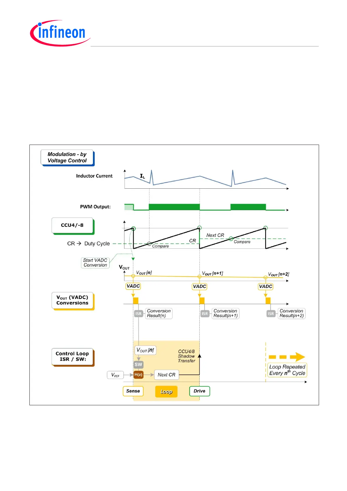
6.1.1 Timing Scheme
The PWM is generated by a CCU4/8 timer in compare mode.
A Compare Register (CR) controls the duty-cycle (D).
The “sense-loop-drive” process (marked by a yellow background in the following figure) is repeated
with a time constant of n loop cycles, while the sensing and averaging of V
OUT
is processed each
cycle.
In Voltage Control (VC) mode there is no need for sensing the inductor current (I
L
). The curve of this
current is shown though, to suggest the preferable PWM events that should start VADC conversions.
Figure 40 Modulation – Voltage Mode Control Timing Scheme

 Loading...