Introduction to Digital Power Conversion
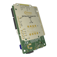
XMC4000/1000 Family
Control Loops
Application Guide 84 V1.0, 2015-01
7.4.1 Open Loop Gain Voltage Mode
The voltage mode control is a relatively slow loop, due to the 2
nd
order low pass filter (H
LP
), the
inductor (L), capacitor (C) and output load (R).
Other transfer functions in the loop are:
DC gain in an ADC (H
ADC
) and (H
DC
) term
A high-frequency function (H
HF
)
A frequency compensation (H
III
)
Figure 68 Voltage Mode Control Open Loop Gain
H
LP
(s)
The cutoff frequency of this 2
nd
order transfer function is
LP
= 1/(LC)
½
. It can be identified as the
‘double-pole’ in the Bode Plot Diagram (Figure 69).
The slope of the absolute value of this 2
nd
order function (as a function of frequency) will fall by 40
dB/decade above the cutoff frequency, until the slope hits the ESR (Equivalent Serial Resistance)
point frequency, after which the slope will be reduced to 20 dB/decade.
ESR
The ESR (Equivalent Serial Resistance) is represented by the resistor (R
C
), as the real component of
the capacitor (C) impedance at high frequencies. The transfer function H
LP
(s) contains a zero at
1/R
C
C in the frequency domain. This zero will erase the effect of one pole in the double-pole.
H
DC
(s)
The DC gain concerns the ratio of VADC resolution to the PWM resolution (It is assumed that the
VADC conversion delay, as well as the data transfer delay by software, is regarded as negligible).
H
HF
(s)
This is the same type of high-frequency 2
nd
order transfer function as for all switch mode converters,
with a double-pole at half the switch frequency (½ f
SW
); i.e.
HF
= /T
SW
(See Figure 69).
 Loading...