Introduction to Digital Power Conversion
XMC4000/1000 Family
Control Loops
Application Guide 85 V1.0, 2015-01
H
III
(s)
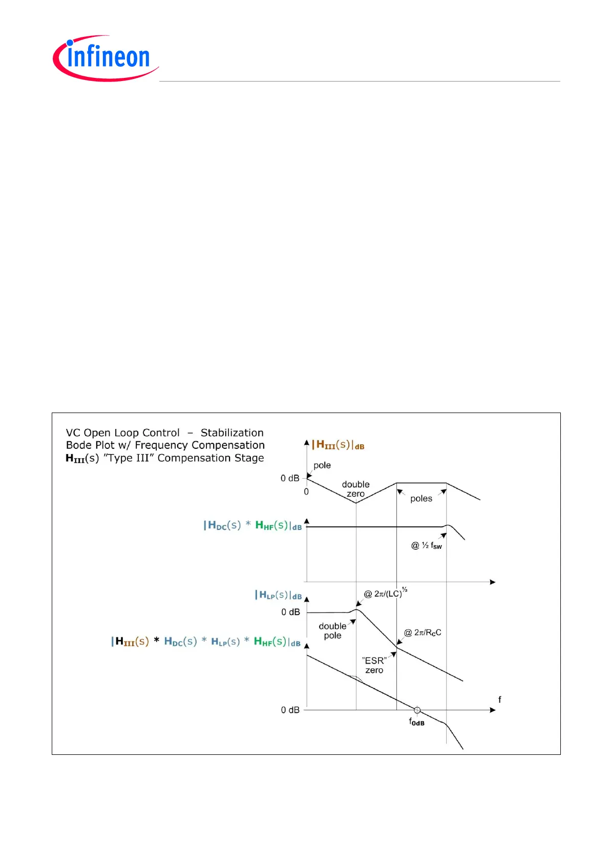
The frequency compensation needs 3 poles and a double-zero to accomplish a nearly 20-dB/decade
slope at the 0-dB level crossing point, for stability, by an appropriate phase margin and damping
factor.
7.4.2 Open Loop Gain Bode Plot, Voltage Mode Stabilization
The voltage mode control open loop gain is a product of the following transfer functions:
H
ADC
(s) * H
III
(s) * H
DC
(s) * H
HF
(s) * H
LP
(s)
(Assume H
ADC
(s) = 1)
Bode-Plot
The vertical co-ordinate of the Bode-Plot diagram is logarithmic in dB (decibel) scale.
The absolute value of the total transfer function will be plotted according to:
|H
III
(s) * H
DC
(s) * H
HF
(s) * H
LP
(s)|
dB
This may also be expressed as:
|H
III
(s)|
dB
+ |H
DC
(s)|
dB
+ |H
HF
(s)|
dB
+ |H
LP
(s)|
dB
(See also Figure 69).
These additions give the Bode-plots:
Figure 69 Voltage Mode Control Open Loop Gain – w/ Frequency Compensation
Note: The H
III
(s) is a Type-III filter and can be realized by software in XMC devices (with software
Library support).
 Loading...