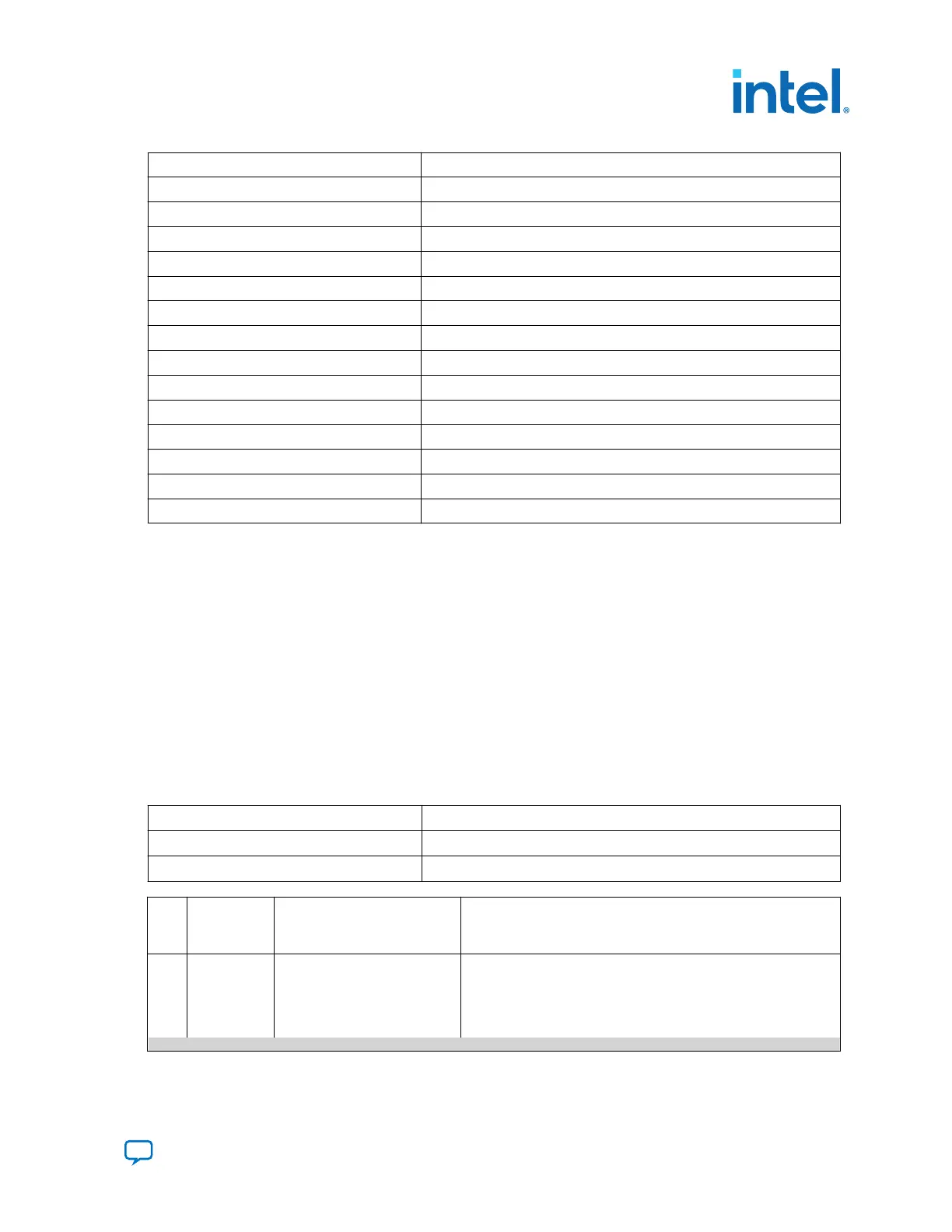
Connector/Switch Description
J16 1PPS IN CONN
J14 1PPS OUT CONN
J56 CY7C68013A I2C CONN
J11 JTAG CONN
J10 USB2.0 CONN
J154 12V HOTSWAP I2C CONN
S19 JTAG SEL SW
S20 MSTR SW
S21 PMBUS_I2C SW
S9 MODE SEL SW
S22 MUX_DIP_SW
S10,S15 SYSTEM SW
S6,S1 USER SW
S7 BOARD POWER ON/OFF SW
A.2. System Management
Two Intel MAX 10 FPGAs (10M16SCU324C8G) are used for system management.
System Intel MAX 10 acts as system controller. It handles FPGA AvST configuration,
I2C bus access, fan speed control and system reset functions. The UB2/PWR Intel MAX
10 acts as Power manager and on-board JTAG controller. Refer to below description for
each function:
• Power management: Control systems and FPGA power up and optional down
sequence, supervise power regulators/switches status and manage power faults,
supervise temperature sensor interrupt signals and manage temperature faults.
• JTAG controller: Manage JTAG chain topology, JTAG master source and JTAG
slaves by S19.
Table 7. JTAG Master Sources
Schematic Signal Name Description
EXT_JTAG_TCK/TDO/TMS/TDI
JTAG header J11 for Intel download cable
FX2_Dp/n
Input port J10 for on-board Intel download circuit
Mode S20[4:1] S19 [4][3] [2] [1]
On: bypass from chain
Off: enable in chain
Function
000 ON/ON/ON
(Default)
S19.1 (SDM+HPS)
S19.2 (SysMax)
S19.3(FMC_B)
S19.4 (FMC_A)
Mode 1: On-board Intel download circuit act as the only JTAG
Master.
Chained HPS with SDM nodes internally.
Mode 3: External Intel download cable act as the only JTAG
Master.
continued...
A. Development Kit Components
776646 | 2023.05.31
Send Feedback
Intel Agilex
®
7 FPGA I-Series Transceiver (6 × F-Tile) Development Kit User
Guide
35

 Loading...


