In systolic FIR mode, the input of the multiplier can come from four different sets of
sources:
• Two dynamic inputs
• One dynamic input and one coefficient input
• One coefficient input and one pre-adder output
• One dynamic input and one pre-adder output
3.1.5.1. Mapping Systolic Mode User View to Variable Precision Block
Architecture View
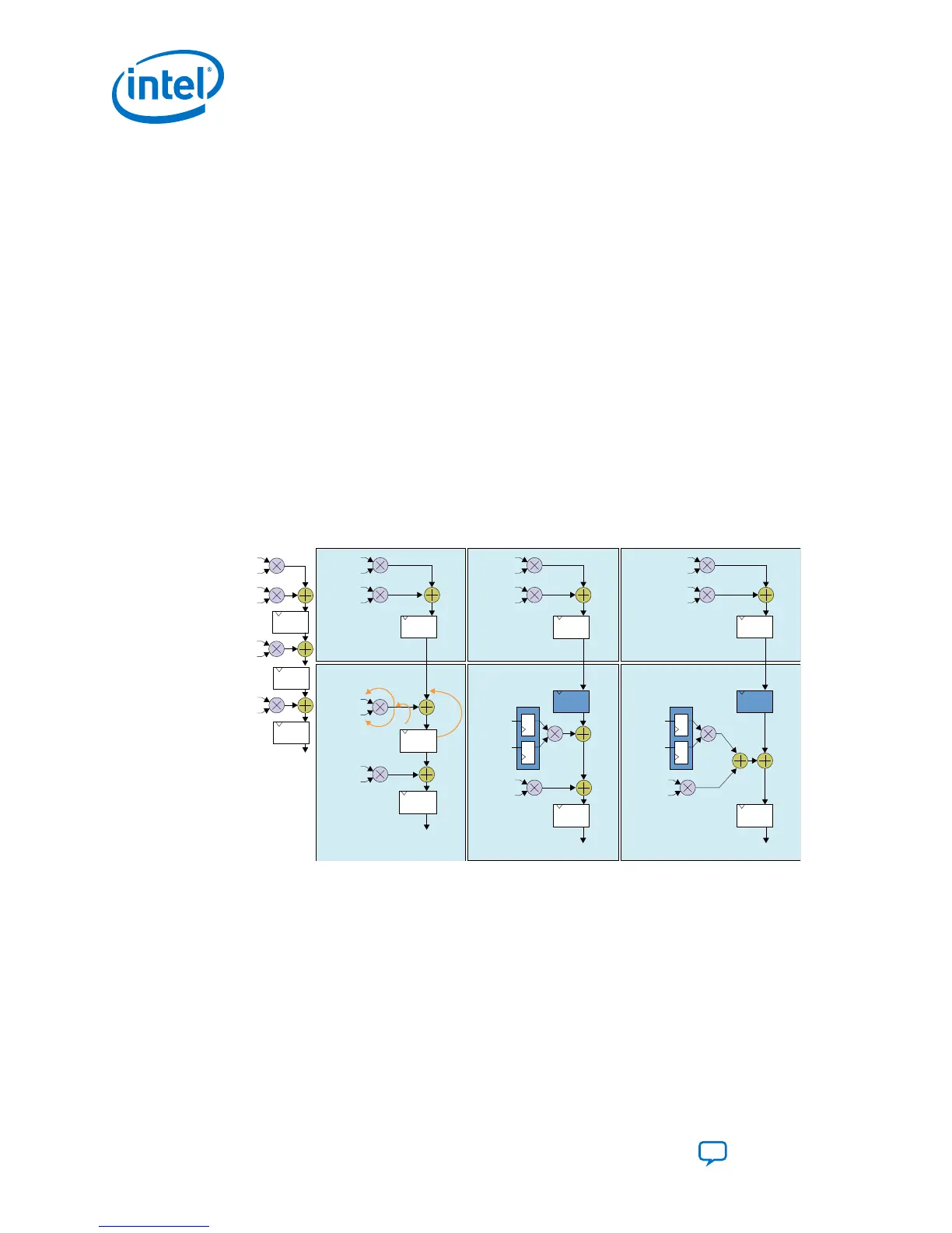
The following figure shows implementation of the systolic FIR filter (a) using the Intel
Agilex variable precision DSP blocks (d) by retiming the register and restructuring the
adder. Register B can be retimed into systolic registers at the chainin, ay and ax input
paths as shown in (b). The end result of the register retiming is shown in (c). The
location of the adder is then restructured to sum both the multipliers output. The
adder result is send to chainout adder to sum with the chainin value from the previous
DSP block as shown in (d).
Figure 25. Mapping Systolic Mode User View to Variable Precision Block Architecture
View
x[n]
c1
(a) Systolic FIR Filter
User View
(b) Variable Precision Block
Architecture View (Before Retiming)
Second DSP Block
dataa_y0 x[n]
dataa_x0 c1
datab_y1 x[n-2]
datab_x1 c2
w1[n]
w2[n]
dataa_y0 x[n-4]
dataa_x0 c3
w3[n]
Register B
datab_y1 x[n-6]
datab_x1 c4
w4[n]
Register C
y[n]
Register A
Multiplier
Multiplier
Adder
Output
Register
Bank
Result
First DSP Block
Result
Output
Register
Bank
Retiming
Chainout
Adder
Chainin from
Previous DSP Block
(c) Variable Precision Block
Architecture View (After Retiming)
Second DSP Block
dataa_y0 x[n]
dataa_x0 c1
datab_y1 x[n-2]
datab_x1 c2
w1[n]
w2[n]
dataa_y0 x[n-4]
dataa_x0 c3
w3[n]
Register B
datab_y1 x[n-6]
datab_x1 c4
w4[n]
Register C
y[n]
Register A
Multiplier
Multiplier
Adder
Output
Register
Bank
Result
First DSP Block
Result
Output
Register
Bank
Chainout
Adder
Chainin from
Previous DSP Block
Systolic
Register
Systolic
Registers
(d) Variable Precision Block
Architecture View (Adder Restructured)
Second DSP Block
dataa_y0 x[n]
dataa_x0 c1
datab_y1 x[n-2]
datab_x1 c2
w1[n]
w2[n]
dataa_y0 x[n-4]
dataa_x0 c3
w3[n]
Register B
datab_y1 x[n-6]
datab_x1 c4
w4[n]
Register C
y[n]
Register A
Multiplier
Multiplier
Adder
Output
Register
Bank
Result
First DSP Block
Result
Output
Register
Bank
Chainout
Adder
Chainin from
Previous DSP Block
Systolic
Register
Systolic
Registers
Adder
x[n-2]
c2
w1[n]
w2[n]
x[n-4]
c3
w3[n]
x[n-6]
c4
w4[n]
y[n]
Register B
Register A
Register A
3.1.5.2. 18-bit Systolic FIR Mode
In 18-bit systolic FIR mode, the adders are configured as dual 44-bit adders, thereby
giving 7 bits of overhead when using an 18 x 19 operation mode, resulting 37-bit
result. This allows a total sixteen 18 x 19 multipliers or eight Intel Agilex variable
precision DSP blocks to be cascaded as systolic FIR structure.
3. Intel Agilex Variable Precision DSP Blocks Operational Modes
UG-20213 | 2019.04.02
Intel
®
Agilex
™
Variable Precision DSP Blocks User Guide
Send Feedback
38
 Loading...