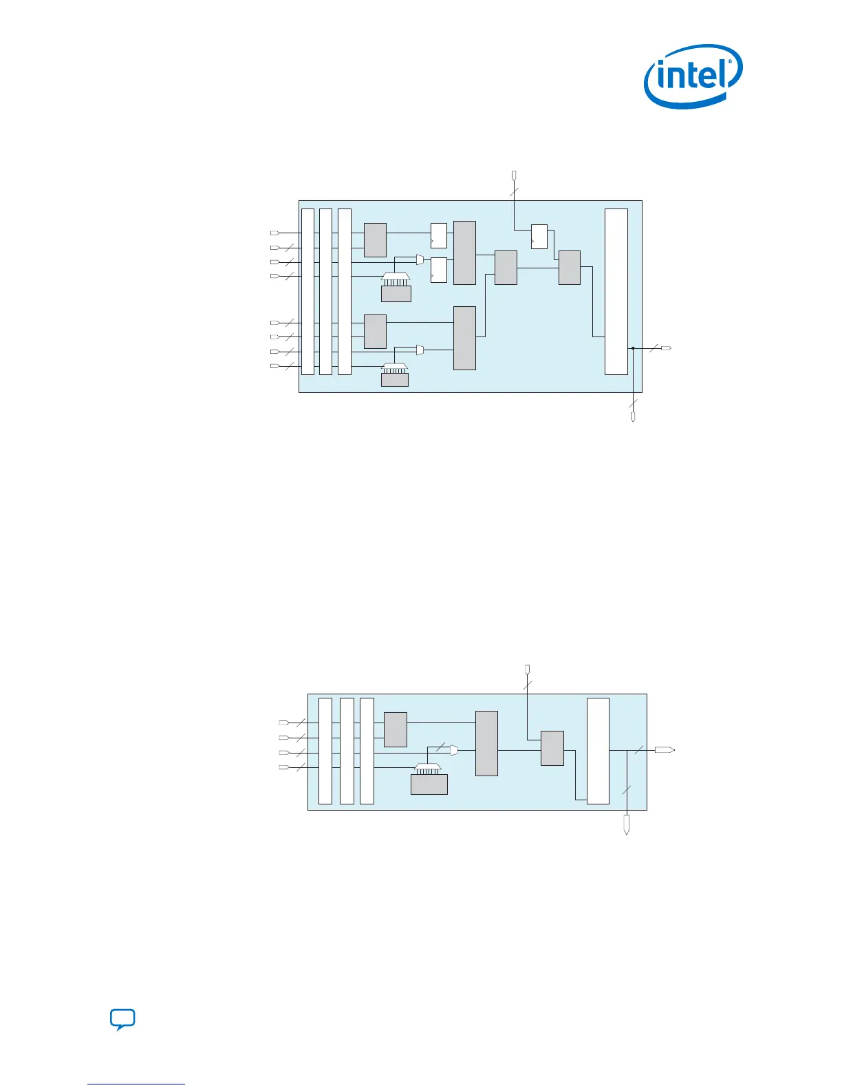
Figure 26. 18-Bit Systolic FIR Mode for Intel Agilex Devices
Input Register Bank
ay[18..0]
az[17..0]
ax[17..0]
COEFSELA[2..0]
by[18..0]
bz[17..0]
bx[17..0]
COEFSELB[2..0]
+/-
Pre-Adder
+/-
Pre-Adder
+/-
Internal
Coefficient
Internal
Coefficient
Multiplier
Multiplier
Adder
+/-
Systolic
Registers
Systolic
Register
Chainout adder or
accumulator
+
Output Register Bank
chainin[43..0]
chainout[43..0]
resulta[43..0]
18-bit Systolic FIR
x
x
19
18
18
19
18
18
3
3
44
44
44
*1st Pipeline Register
*2nd Pipeline Register
*This block diagram shows the functional representation of the DSP block.
The pipeline registers are embedded within the various circuits of the DSP block.
Systolic
Registers
3.1.5.3. 27-Bit Systolic FIR Mode
In 27-bit systolic FIR mode, the chainout adder or accumulator is configured for a
64-bit operation, providing 10 bits of overhead when using a 27-bit data (54-bit
products). This allows a total of eleven 27 x 27 multipliers or eleven Intel Agilex
variable precision DSP blocks to be cascaded as systolic FIR structure.
The 27-bit systolic FIR mode allows the implementation of one stage systolic filter per
DSP block. Systolic registers are not required in this mode.
Figure 27. 27-Bit Systolic FIR Mode for Intel Agilex Devices
Input Register Bank
ay[25..0]
az[25..0]
ax[26..0]
COEFSELA[2..0]
Pre-Adder
+/-
Internal
Coefficient
Multiplier
Chainout adder or
accumulator
+
chainin[63..0]
chainout[63..0]
27-bit Systolic FIR
27
x
Output Register Bank
26
3
27
26
64
64
*2nd Pipeline Register
*1st Pipeline Register
64
resulta[63..0]
*This block diagram shows the functional representation of the DSP block.
The pipeline registers are embedded within the various circuits of the DSP block.
3. Intel Agilex Variable Precision DSP Blocks Operational Modes
UG-20213 | 2019.04.02
Send Feedback
Intel
®
Agilex
™
Variable Precision DSP Blocks User Guide
39
 Loading...