Electrical Specifications
24 Quad-Core Intel® Xeon® Processor 5300 Series Datasheet
2.7 Front Side Bus Signal Groups
The FSB signals have been combined into groups by buffer type. AGTL+ input signals
have differential input buffers, which use GTLREF_DATA_MID, GTLREF_DATA_END,
GTLREF_ADD_MID, and GTLREF_ADD_END as reference levels. In this document, the
term “AGTL+ Input” refers to the AGTL+ input group as well as the AGTL+ I/O group
when receiving. Similarly, “AGTL+ Output” refers to the AGTL+ output group as well as
the AGTL+ I/O group when driving. AGTL+ outputs can become active anytime and
include an active PMOS pull-up transistor to assist during the first clock of a low-to-high
voltage transition.
With the implementation of a source synchronous data bus comes the need to specify
two sets of timing parameters. One set is for common clock signals whose timings are
specified with respect to rising edge of BCLK0 (ADS#, HIT#, HITM#, etc.) and the
second set is for the source synchronous signals which are relative to their respective
strobe lines (data and address) as well as rising edge of BCLK0. Asynchronous signals
are still present (A20M#, IGNNE#, etc.) and can become active at any time during the
clock cycle. Table 2-6 identifies which signals are common clock, source synchronous
and asynchronous.
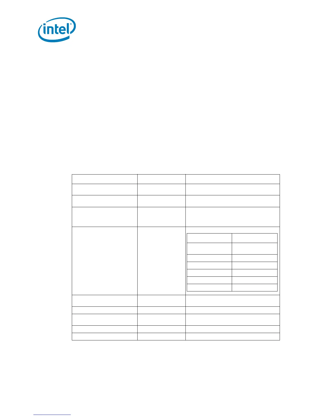
Table 2-6. FSB Signal Groups (Sheet 1 of 2)
Signal Group Type Signals
1
AGTL+ Common Clock Input Synchronous to
BCLK[1:0]
BPRI#, DEFER#, RESET#, RS[2:0]#, RSP#,
TRDY#;
AGTL+ Common Clock Output Synchronous to
BCLK[1:0]
BPM4#, BPM[2:1]#, BPMb[2:1]#
AGTL+ Common Clock I/O Synchronous to
BCLK[1:0]
ADS#, AP[1:0]#, BINIT#
2
, BNR#
2
, BPM5#,
BPM3#, BPM0#, BPMb3#, BPMb0#, BR[1:0]#,
DBSY#, DP[3:0]#, DRDY#, HIT#
2
, HITM#
2
,
LOCK#, MCERR#
2
AGTL+ Source Synchronous I/O Synchronous to assoc.
strobe
AGTL+ Strobes I/O Synchronous to
BCLK[1:0]
ADSTB[1:0]#, DSTBP[3:0]#, DSTBN[3:0]#
Open Drain Output Asynchronous FERR#/PBE#, IERR#, PROCHOT#, THERMTRIP#
CMOS Asynchronous Input Asynchronous A20M#, FORCEPR#, IGNNE#, INIT#, LINT0/
INTR, LINT1/NMI, PWRGOOD, SMI#, STPCLK#,
CMOS Asynchronous Output Asynchronous BSEL[2:0], VID[6:1]
FSB Clock Clock BCLK[1:0]
Signals Associated Strobe
REQ[4:0]#,A[16:3]#,
A[37:36]#
3
ADSTB0#
A[35:17]# ADSTB1#
D[15:0]#, DBI0# DSTBP0#, DSTBN0#
D[31:16]#, DBI1# DSTBP1#, DSTBN1#
D[47:32]#, DBI2# DSTBP2#, DSTBN2#
D[63:48]#, DBI3# DSTBP3#, DSTBN3#