Electrical Specifications
42 Quad-Core Intel® Xeon® Processor 5300 Series Datasheet
6. GTLREF should be generated from V
TT
with a 1% tolerance resistor divider. The V
TT
referred to in these
specifications is the instantaneous V
TT
.
7. Specified when on-die R
TT
and R
ON
are turned off. V
IN
between 0 and V
TT
.
8. This is the measurement at the pin.
Notes:
1. Unless otherwise noted, all specifications in this table apply to all processor frequencies.
2. The V
TT
referred to in these specifications refers to instantaneous V
TT
.
3. Refer to the processor I/O Buffer Models for I/V characteristics.
4. Measured at 0.1*V
TT
.
5. Measured at 0.9*V
TT
.
6. For Vin between 0 V and V
TT
. Measured when the driver is tristated.
7. This is the measurement at the pin.
Notes:
1. Unless otherwise noted, all specifications in this table apply to all processor frequencies.
2. Measured at 0.2*V
TT
.
3. V
OH
is determined by value of the external pullup resistor to V
TT
. Please refer to platform design guide for
details.
4. For V
IN
between 0 V and V
OH
.
5. This is the measurement at the pin.
2.13.2 V
CC
Overshoot Specification
Processors can tolerate short transient overshoot events where V
CC
exceeds the VID
voltage when transitioning from a high-to-low current load condition. This overshoot
cannot exceed VID + V
OS_MAX
(V
OS_MAX
is the maximum allowable overshoot above
VID). These specifications apply to the processor die voltage as measured across the
VCC_DIE_SENSE and VSS_DIE_SENSE lands and across the VCC_DIE_SENSE2 and
VSS_DIE_SENSE2 lands.
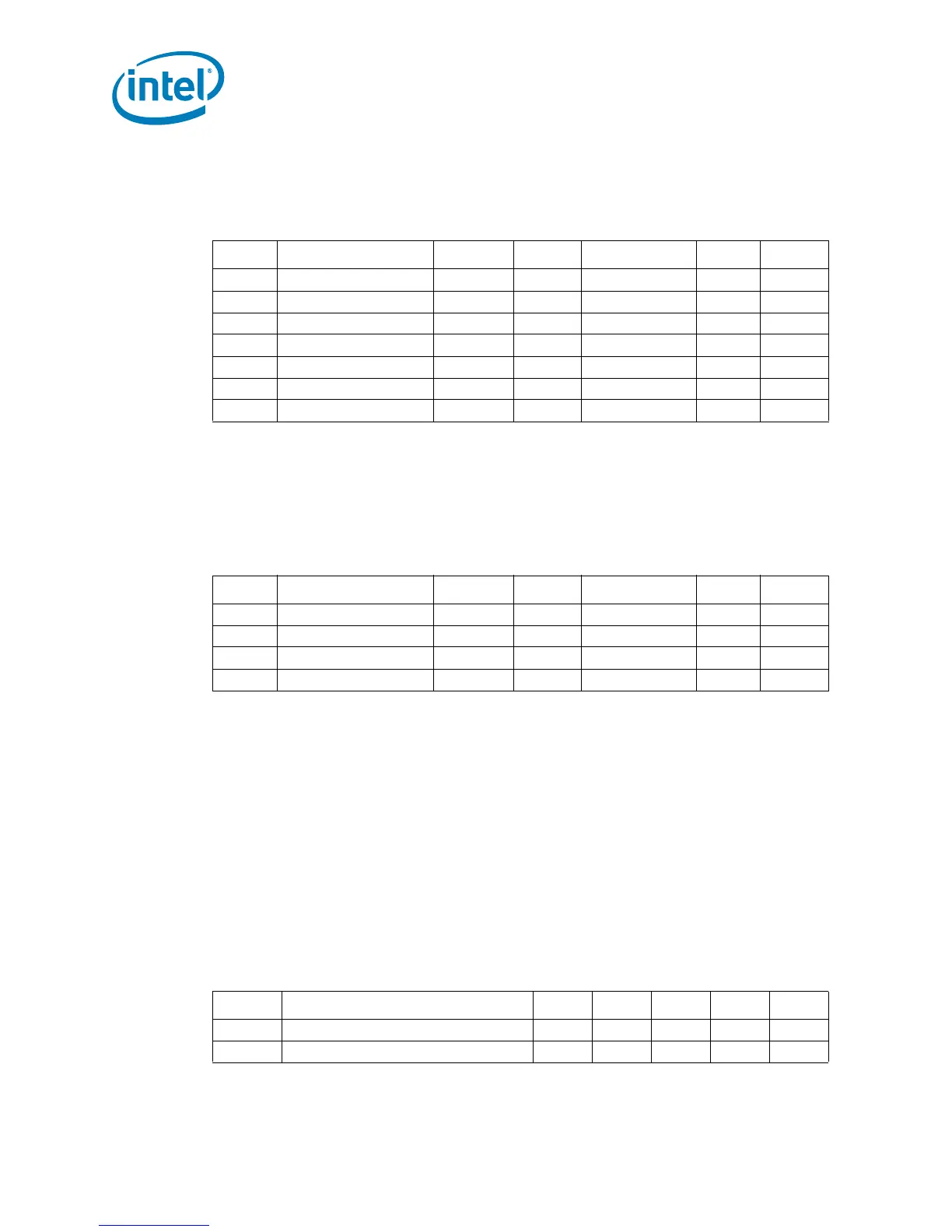
Table 2-17. CMOS Signal Input/Output Group and TAP Signal Group DC Specifications
Symbol Parameter Min Typ Max Units Notes
1
V
IL
Input Low Voltage -0.10 0.00 0.3*V
TT
V2,3
V
IH
Input High Voltage 0.7*V
TT
V
TT
V
TT
+0.1 V 2
V
OL
Output Low Voltage -0.10 0 0.1*V
TT
V2
V
OH
Output High Voltage 0.9*V
TT
V
TT
V
TT
+0.1 V 2
I
OL
Output Low Current 1.70 N/A 4.70 mA 4
I
OH
Output High Current 1.70 N/A 4.70 mA 5
I
LI
Input Leakage Current N/A N/A ± 200 μA6,7
Table 2-18. Open Drain Output Signal Group DC Specifications
Symbol Parameter Min Typ Max Units Notes
1
V
OL
Output Low Voltage N/A 0.20 V
V
OH
Output High Voltage 0.95 * V
TT
V
TT
1.05 * V
TT
V3
I
OL
Output Low Current 16 N/A 50 mA 2
I
LO
Leakage Current N/A N/A ± 400 μA4,5
Table 2-19. V
CC
Overshoot Specifications
Symbol Parameter Min Max Units Figure Notes
V
OS_MAX
Magnitude of V
CC
overshoot above VID 50 mV 2-12
T
OS_MAX
Time duration of V
CC
overshoot above VID 25 µs 2-12