Keysight N5221A/22A Service Guide 5-23
Theory of Operation
Receiver Group Operation
A12 SPAM Board (Analog Description)
The A12 SPAM board contains digital and analog circuitry. For digital
descriptions, refer to “A12 SPAM Board (Digital Description)” on page 5-29.
In this assembly, the IF signals (A, B, C, D, and R for 4-port models and A, B,
R1, and R2 for 2-port models) from the A20 IF multiplexer board go through a
gain stage where small signals are amplified to ensure that they can be
detected by the analog-to-digital converter (ADC).
All input signals are sampled simultaneously by the ADCs, where they are
converted to digital form. The ADC conversions are triggered by timing signals
from the digital signal processor (DSP) in response to commands from the
central processing unit (CPU). The digitized data is processed into magnitude
and phase data by the DSP and sent to the CPU random access memory (RAM)
by way of the peripheral component interconnect (PCI) bus.
The processed and formatted data is finally routed to the display, and to the
general-purpose interface bus (GPIB) for remote operation. Refer to “Digital
Processing and Digital Control Group Operation” on page 5-26 for more
information on signal processing.
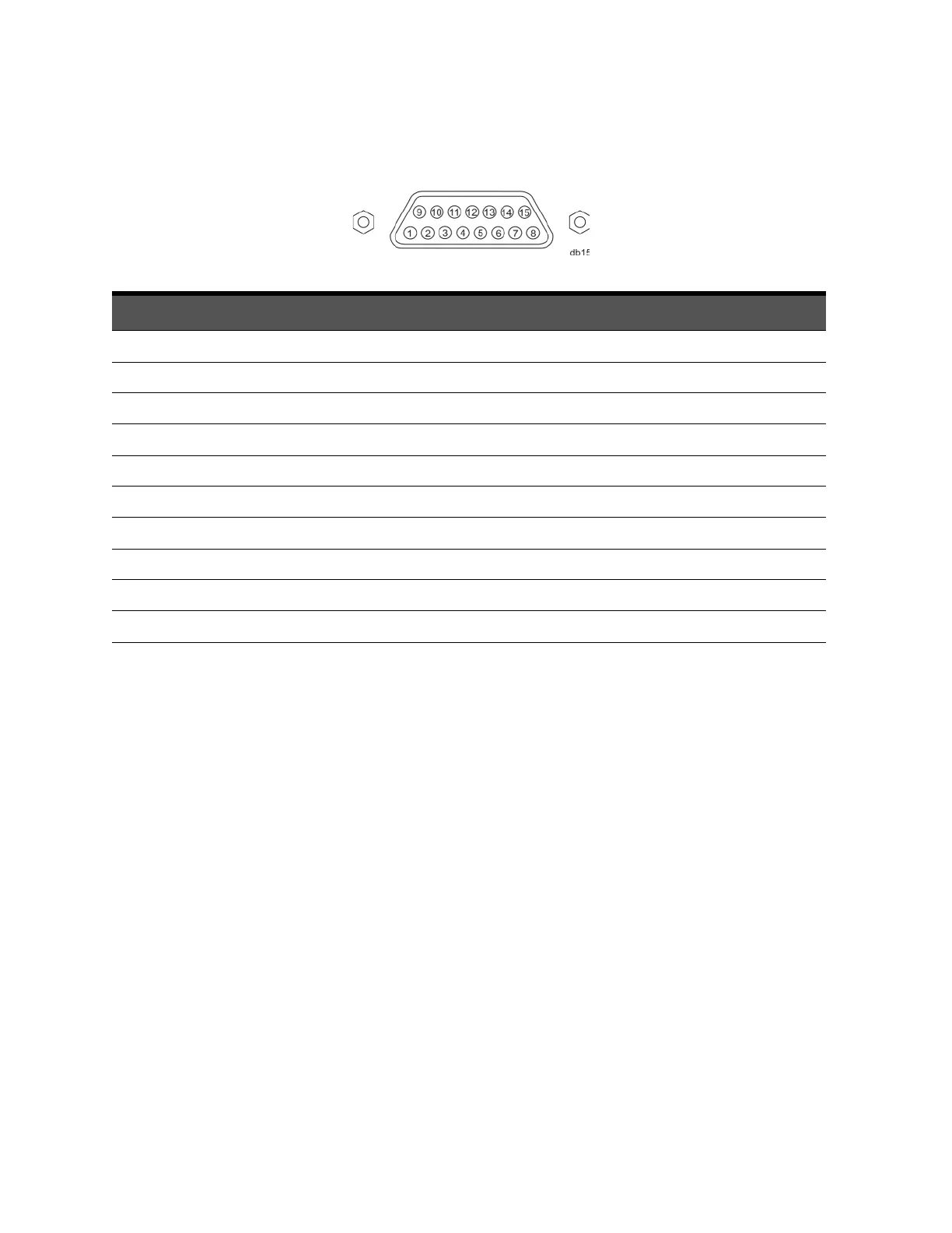
6 DCOM Digital ground
7 PulseSyncIn Pulse generator synchronization trigger input (TTL)
8 RFPulseModIn RF source pulse modulation drive input (TTL)
9 DCOM Digital ground
10 Pulse1Out Programmable pulse train output #1 (TTL)
11 Pulse2Out Programmable pulse train output #2 (TTL)
12 Pulse3Out Programmable pulse train output #3 (TTL)
13 Pulse4Out Programmable pulse train output #4 (TTL)
14 NC No connect
15 DCOM Digital ground
Table 5-4 PULSE I/O Connector Pin Assignments
DB-15 Female Connector
Pin Name Description