8-11
z Normal PID drive (H54=0)
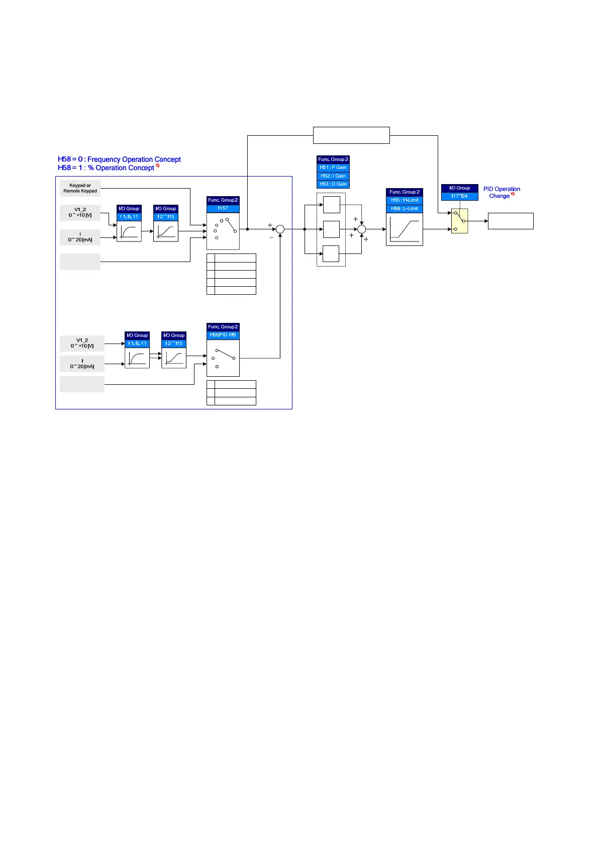
PID control diagram
0
1
2
PID F/B Select
Communi-
cation
3)
K
P
K
I
/s
K
D
s
PID Gain
PID Limit
Analog Input
Filter
Analog Input
Scale
V1_2 : 0 ~ 10V
I : 0 ~ 20mA
1
0
2 Communication
PID Command
Select
Communi-
cation
Analog Input
Filter
Analog Input
Scale
Keypad Setting 2
V1_2 : 0 ~ 10V
I : 0 ~ 20mA
1
2
3
4
Keypad Setting 10
Communication
PID REF
4)
PID FBK
5)
Frequency Conversion
6)
PID Output
Frequency
7)
0
1
2
3
4
PID OUT
8)
Mult Function
Input
3) Adds RS-485 communications to PID Feedback category.
4) PID REF value can be changed and checked in the “rEF” of the DRV group.
Unit is [Hz] when H58=0 and [%] when H58=1
5) PID FBK value cab be checked in the “Fbk” of the DRV group
Unit is sane with the “rEF”
6) If PID switching is inputted to the multi-input (P1~P8), though H58 is 1, [%] is converted into [Hz].
7) Output frequency is displayed in the “SPD” of DRV group.
8) PID OUT of Normal PID is single polarity and it is limited by H55 (H-Limit) and H56 (L-Limit).
9) 100% is F21 (Max. frequency)
 Loading...